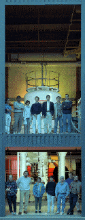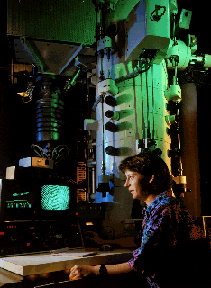


THE PAIR OF BLUE TOWERS RISING TO A height of nearly 100 feet have become a Strawberry Canyon landmark. Inside those towers are the two electron microscopes that blazed a trail for the rest of the world to follow. In celebrating the tenth anniversary of the National Center for Electron Microscopy (NCEM), the LBL staff there can take pride in a storied past and look forward to an even better future.
Constructed at a cost of $7.5 million, NCEM was officially dedicated on September 30, 1983. That date also marked the unveiling of the Atomic Resolution Microscope (ARM), the first instrument in the world capable of showing individual atoms in a sample. ARM joined the High Voltage Electron Microscope, which had been in operation since 1981, to give NCEM an unprecedented one-two technological punch that each year draws users from across the nation and around the globe. Among these users are industrial researchers with such high-tech giants as IBM, Intel, Hewlett-Packard, General Motors and Xerox; university researchers from such leading institutes as MIT, Cal Tech, Georgia Tech, Stanford, and Carnegie-Mellon; and federal researchers from sister national laboratories and from other top government science agencies such as NASA and NIST.
These and other users are drawn to NCEM like pilgrims to Mecca because electron microscopy has become the keystone in materials sciences. A highly skilled blend of science, art, and technical craft, with maybe just a touch of luck, this arcane field has led to the solving of material failure problems that in the past caused bridges to collapse, planes to crash, waste containment vessels to leak, and hosts of other less dramatic but still very important incidents. Electron microscopy has also led to the development of new materials and technologies that have advanced the fields of manufacturing, communications, transportation, and data processing. In many of these achievements, NCEM played a central role.
NCEM was started by LBL metallurgist Gareth Thomas, who became the scientific director of the facility when it opened. Another LBL scientist, Ken Westmacott, became NCEM's first managing director. Both Thomas and Westmacott retired from their respective duties in 1991. The two jobs were combined and Uli Dahmen, a materials scientist and engineer, and an expert in microstructure crystallography, took over.
"Gareth Thomas provided the vision that got NCEM started and Ken Westmacott established the infrastructure that made it the premier facility of its kind," Dahmen says. "My mission is to keep us at the scientific forefront."
The electron microscope was invented in 1931 by German physicist Ernst Ruska while he was working on the development of an oscilloscope. Its operation is similar to that of a conventional microscope except that instead of shooting visible light through a specimen, it shoots a beam of fast-moving electrons. Because electrons have a much shorter wavelength than visible light photons, they can be used to "resolve" or bring into view much smaller things. For example, whereas the best visible light microscopes magnify objects some 2,000 times, today's best electron microscopes can magnify objects a million times or more.


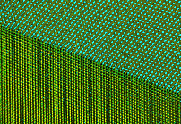
Left, a three-dimensional view of the atomic structure of the mineral staurolite, revealing the positions of the silicon, aluminum, and oxygen atoms. Right, an atomic resolution micrograph of an interface between aluminum and germanium.
"You won't find the things available here duplicated elsewhere in the country," Thomas declared at the time NCEM opened. In the following years, his case was made even stronger. The HVEM was equipped with a special sample chamber that made it possible for scientists to study specimens during heating, cooling, straining, or exposure to controlled but realistic atmospheric conditions. The ARM's performance was enhanced with the addition of a high-angle "tilt stage" that allows full resolution images to be obtained along any axis through a sample -- something no other electron microscope offers. Both microscopes were further complemented (and their overall performances improved) with new advanced computer systems for sophisticated image simulations and faster electron micrograph processing to enable researchers to correctly interpret the structures being imaged. The software developed at NCEM has been widely distributed to other electron microscope labs.
Finally, a third major microscope was added to the NCEM family, the Analytical Electron Microscope (AEM), a smaller instrument -- 200,000 electron volt (200 keV) -- equipped with a special x-ray detector as well as other features to provide information on chemical composition and on atomic structure and bonding. The AEM can be used independently or in conjunction with the ARM or the HVEM.