|
|
 |
Using "stage machinery" unique to the
Advanced Light Source, a cast of players from Berkeley Lab, IBM
Corporation, Stanford University, and other institutions are mounting what
one of their number, Frithjof Nolting, calls "an opera in many
acts" -- an opera that goes by the title Secrets of
Antiferromagnetism.
Not as catchy as The Magic Flute, but a lot more practical:
antiferromagnetism is a phenomenon vital to the layered structures of
today's advanced computer hard-disk read heads and to the memory devices
of the future.
 |

THE FRONT LAYER IN THIS READ HEAD (GREEN) IS A FERROMAGNET WHOSE
MAGNETIC DOMAINS ARE FREE TO RESPOND TO THE EXTERNAL FIELD OF A BIT
PASSING BENEATH ON THE HARD DISK. IN THE SECOND FERROMAGNETIC
LAYER, DOMAINS ARE PINNED BY THE ANTIFERROMAGNET IN BACK. WHEN THE
DOMAINS IN THE FERROMAGNETIC LAYERS ARE ORIENTED DIFFERENTLY,
ELECTRICAL RESISTANCE INCREASES GREATLY.
Image courtesy of IBM Corp.
|
"A modern read head uses layers of very thin films with different
magnetic properties," explains Andreas Scholl of the ALS. "As
the head passes over the hard disk, these layers sense the orientation of
the domains on the disk and cause the head's electrical resistance to
change in response."
At normal temperatures, the electronic spins in the magnetic domains of
ferromagnetic materials such as iron or cobalt are parallel and point in
the same direction; the domains change their orientation in the presence
of an applied magnetic field. A read head takes advantage of the fact that
if two ferromagnetic layers share the same orientation, they exhibit less
electrical resistance than when they are opposed.
While spins in the magnetic domains of antiferromagnetic materials are
also parallel, they alternately point in opposite directions, so on
average the material is insensitive to applied magnetic fields. This comes
in handy for read heads: in order for one of the ferromagnetic layers in a
read head to switch independently of the other, one of them must be
"pinned" by an underlying antiferromagnetic layer.
The more formal term for pinning is "exchange bias" -- a
phenomenon known for more than 45 years. "Even though we have used
the effect and even built devices by trial and error, we haven't
understood how it works," says Frithjof Nolting, an ALS researcher
visiting from Stanford University.
Two things were needed for a better understanding, Nolting says:
"first, a method of imaging the configuration of domains in
antiferromagnetic thin films, which requires a resolution better than 100
nanometers" (100 billionths of a meter) "and second, a way to
image the interface between ferromagnetic and antiferromagnetic domains in
adjacent layers," which requires distinguishing between layers
containing different chemical elements.
"The only method that can do all this is photo-electron emission
microscopy, or PEEM," says Simone Anders, leader of the team that
built the PEEM2 microscope on ALS beamline 7.3.1.1. When an x-ray beam is
incident upon a sample, PEEM2 uses electrons ejected from the sample to
form an image with ten-thousand-fold magnification and a resolution of 20
nanometers.
X-rays of different energies stimulate photoelectrons characteristic of
different elements; thus by tuning the energy of the beam, layers
containing different elements can be distinguished. And if the beam is
polarized, it can reveal magnetic domains: linear polarization yields
images of antiferromagnetic domains, while circular polarization reveals
ferromagnetic domains.
 |

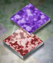
IMAGES MADE BY THE PEEM2 MICROSCOPE SHOW
THAT AT THE INTERFACE OF A THIN LAYER OF COBALT, A FERROMAGNET, AND
LANTHANUM IRON OXIDE, AN ANTIFERROMAGNET, MAGNETIC DOMAINS ARE
PRECISELY ALIGNED.
|
With PEEM2 in place at the ALS, the curtain was set to rise. Act 1
appeared in Science magazine this February, when the researchers
reported the first images that clearly revealed the alignment of domains
in an antiferromagnetic thin film. When these PEEM2 images, each only a
few hundred nanometers in area, were compared to transmission electron
microscope images of the same sample, the magnetic domains corresponded
exactly to the orientation of its crystals.
Act 2 was a letter to Nature in June, when the researchers
announced another first: direct images of the alignment of magnetic
domains on both sides of an interface between ferromagnetic and
antiferromagnetic layers.
In this work the sample was a ferromagnetic cobalt film, less than
three nanometers thick, deposited on a film of antiferromagnetic lanthanum
iron oxide. "By tuning the photon energy of the beam, we were able to
record separate images of the antiferromagnetic and ferromagnetic layers
in exactly the same place," Nolting says.
The perfectly registered images show precise correspondence between the
spin orientation of microscopic domains in the lanthanum iron oxide layer
and the domains of the cobalt layer immediately adjacent to them,
demonstrating that exchange coupling aligns the magnetic structure of both
layers, domain by domain.
But the end of Act 2 held a surprise: when the researchers measured the
strength of the coupling by applying a magnetic field, they discovered an
unexpected phenomenon.
Because exchange-bias devices such as read heads depend upon an overall
preferred magnetic orientation in a ferromagnetic layer coupled to an
antiferromagnet layer, a "bias" is set during the manufacturing
process.
"The usual method is to set a bias by annealing the multilayer in
a magnetic field," Nolting explains, which takes advantage of the
fact that magnetic materials lose their magnetism above a critical
temperature, then regain it as they cool. However, Nolting says, "we
imaged samples just as they were grown, without any additional
processing."
The surpise: "We found that prior to any setting procedure, there
is already a bias locally, within each individual domain. Apparently
exchange bias is an intrinsic property of the interface, caused by the
common alignment of the magnetic structure of both materials, even though
initially there may be no total bias, averaged over a large area."
Says Nolting, "This opens the door to new investigations, which
may affect the way devices based on the exchange bias effect are
manufactured" -- as well as the materials chosen to make them.
Thus the latest plot twist suggests that many more surprises are in
store, in the ongoing drama of antiferromagnetism's secrets.
In addition to Andreas Scholl, Frithjof Nolting and Simone Anders,
other members of the research team are Joachim Stöhr of Stanford
University, formerly of the IBM Almaden Research Center in San Jose, who
led the project; Jin Won Seo of the University of Neuchâtel and IBM's
Zürich Research Laboratory; Jean Fompeyrine, Heinz Siegwart, and
Jean-Pierre Locquet of IBM's Zürich Research Laboratory; Jan Lüning, now
with the Stanford Synchrotron Radiation Laboratory, Eric. E. Fullerton,
and Michael F. Toney of IBM's Almaden Research Center; Michael R.
Scheinfeld of Arizona State University; and Howard A. Padmore of the ALS.
PEEM2 was built under a corporate research and development agreement (CRADA)
between IBM and Berkeley Lab, in collaboration with Arizona State
University.
Additional information:
|


