|
February 10, 2000 |
|
 |
 |
|
|
|
|
BERKELEY, CA ó The PEEM2
microscope, a new x-ray spectromicroscopy facility at the Advanced Light
Source (ALS) located at the Department of Energy's Lawrence Berkeley
National Laboratory, has produced the first images of the domain structure
of an antiferromagnetic thin film -- a type of material vital to advanced
magnetic devices such as the read heads of computer hard-disk drives.
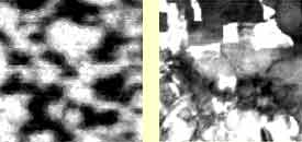
The high-resolution images reveal that the alignment of tiny magnetic domains in lanthanum iron oxide, each only a few hundred nanometers (billionths of a meter) in size, corresponds to a particular orientation of the material's crystals. This and other findings hold promise for the fabrication of improved magnetic devices.
PEEM2 was built under a joint Corporate Research and Development Agreement between the IBM Corporation and Berkeley Lab, in collaboration with Arizona State University. Researchers from the ALS, from IBM Corporation's research centers in San Jose, Calif., and ZŁrich, Switzerland, and from the University of Neuch‚tel and Arizona State University report their achievement in the February 11 issue of the journal Science. "A modern read head uses layers of very thin films with different magnetic properties," explains Andreas Scholl, a member of the Experimental Systems Group at the ALS led by Howard Padmore. "As the head passes over the hard disk, these layers sense the orientation of the domains on the disk and cause the head's electrical resistance to change in response." When the head's ferromagnetic layers share the same magnetic orientation, there is less electrical resistance than when they are magnetically opposed. In order for one layer to switch independently of another, however, one must be "pinned" by an underlying antiferromagnetic layer, which is insensitive to applied magnetic fields. There are many different materials with ferromagnetic and antiferromagnetic properties, "but read heads are constructed from these on a trial-and-error basis," says Joachim StŲhr of the IBM Almaden Research Center in San Jose. "Nobody really knows the mechanism that couples the ferromagnet to the antiferromagnet." To study magnetic materials in microscopic detail, the researchers needed a tool with very high spatial resolution -- and one that was sensitive to the orientation of magnetic and antiferromagnetic domains, sensitive to surfaces and interfaces, and could distinguish one kind of atom from another. "The only method that can do all this is photo-electron emission microscopy -- PEEM -- using an intense beam of monochromatic x rays from a synchrotron light source like the ALS," says Simone Anders, leader of the team that built the PEEM2. A bright beam of x rays focused on a sample in the PEEM2 causes it to emit electrons, which the microscope focuses into an image with a spatial resolution approaching 20 nanometers. The energy of the illuminating beam can be tuned to pick out specific elements -- for example, iron emits electrons with most intensity when the photons in the beam have an energy of about 710 electron volts. The soft x-ray beam can be polarized circularly or linearly. Circular polarization is used to image ferromagnetic materials, whose domains have their magnetic spins aligned in the same direction. To image antiferromagnetic domains, in which spins are aligned opposite to each other, linear polarization is needed. When the electrical axis (E-vector) of the linearly polarized light is parallel to the spin axis in a domain, the beam excites electron emission which shows up brightly on the PEEM2 image; where spins are arranged at right angles to the polarized light's E-vector, the domain shows up as a dark spot. The magnetic structure of the surface can be deduced from these images. "Without samples in which the size and the orientation of the magnetic domains are precisely controlled, we could not have obtained these images," Anders says of the crystals, which were made by Jean-Pierre Locquet's group at IBM's ZŁrich Research Laboratory. "The excellent quality of the ZŁrich samples was essential to the success of the project." Locquet says, "We originally developed this process to grow high-temperature superconductors." Using molecular beam epitaxy, single layers of lanthanum oxide and iron oxide were deposited one after the other to build up the compound. The samples were gradually heated to make sure the images were really due to magnetism and not some other feature of the thin film. The Nťel temperature (like the Curie temperature of other magnetic materials) is the temperature at which antiferromagnetic materials lose magnetism. When the thin film sample was heated in PEEM2, image contrast indeed vanished -- and returned again as the sample cooled -- but whereas in bulk the Nťel temperature of lanthanum iron oxide is 740 degrees Kelvin, in the sample it was only 670 K. "We think that what lowers the Nťel temperature of our lanthanum iron oxide sample is structural deformation," says Jin Won Seo of the University of Neuch‚tel. "It's a film only 40 nanometers thick, laid on a substrate of strontium titanium oxide. When an epitaxial thin film of one material is laid onto a substrate of a different material, it's almost impossible to get the two crystal lattices to match perfectly, and atoms get pushed out of place -- which modifies magnetic properties." Perhaps the most remarkable finding of all came when Seo compared the PEEM2 images of magnetic domains with her transmission electron microscope images of the same sample, acquired at IBM's ZŁrich laboratory. The crystal structure of lanthanum iron oxide (perovskite structure) has a long axis, which lay in the plane of the thin-film sample along two directions at right angles. Both the size and orientation of the sample's crystal domains coincided with its magnetic domains, showing that they are closely correlated. Jean Fompeyrine of the ZŁrich laboratory remarks that this is not only interesting science in its own right, but "it shows us how we can build materials that control the size and orientation of magnetic domains. This understanding will then allow us to develop better read heads." The next step is to study the interface between ferromagnetic and antiferromagnetic materials. Lanthanum iron oxide is an antiferromagnetic material whose domain structure is large enough to be resolved by the PEEM2, but it is not the material used in technological devices. Eric Fullerton of IBM's Almaden Research Center explains that "in current read head devices, more common antiferromagnets like nickel oxide and iron-manganese are used." To study those materials will require higher resolution, however, "which is why PEEM3 is already underway," says the ALS's Simone Anders. Compared to the 20-nanometer resolution of PEEM2, "this improved photo-electron emission microscope will have two-nanometer spatial resolution." "Observation of antiferromagnetic domains in epitaxial thin films" by A. Scholl, J. StŲhr, J. LŁning, J. W. Seo, J. Fompeyrine, H. Siegwart, J.-P. Locquet, F. Nolting, S. Anders, E. E. Fullerton, M. R. Scheinfein, and H. A. Padmore appears in the 11 February 2000 issue of Science. The Berkeley Lab is a U.S. Department of Energy national laboratory located in Berkeley, California. It conducts unclassified scientific research and is managed by the University of California. Additional Information: |