
|
|
|

| "Alex Zettl makes the most incredible devices you'll never see - at least not without the aid of an electron microscope. Zettl, a physicist who holds a joint appointment with Berkeley Lab's Materials Sciences Division (MSD) and the Physics Department of the University of California at Berkeley, has led the creation of what may be the world's smallest human-made bearings and mechanical switches, the world's smallest room-temperature diodes, and a "tube cube" electronic device with the potential to wire itself. These devices have been fashioned from hollow tubular macromolecules only a few nanometers (billionths of a meter) in diameter. Such macromolecules are called "nanotubes" and they have emerged as premier building blocks for the coming age of nanotechnology. |
 |
|
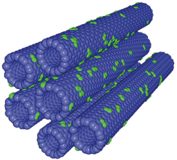
| Single-walled carbon nanotubes are so oxygen-sensitive that the absorption of even a few atoms of oxygen (shown in green) can change semiconducting tubes into conductors. | |
Not only do nanotubes offer a full range of electrical and thermal conductivity properties (they conduct heat better than any other known material), they're also about a hundred times stronger than steel and more durable than diamonds. Their potential for use in electronics is nothing short of mind-boggling: if all the nanotubes that could be packed into a one-half-inch cube were to be laid out end to end, they would stretch some 250,000 miles.
"The most exciting thing is that a lot of structures we are now making in the laboratory and studying are very relevant to everyday life, from being used as structural materials, to electronic materials, to chemical sensing," says Zettl. "In almost any technological application you want to think of, nanotubes probably will have an impact."
Nanotubes are two-dimensional crystalline sheets of atoms that have been rolled up and connected at the seam to form a closed cylinder. The earliest nanotubes were made from pure carbon. Formed naturally in the sooty residue of vaporized carbon rods, they were an elongated form of fullerene or "buckyball" molecules, clusters of 60 and 70 carbon atoms joined in a graphite-like mesh of hexagonal rings. The first generations were "multi-walled nanotubes" (MWNTs): about five to 40 single-walled nanotubes (SWNTs)-meaning the tube's surface consists of only a single layer of carbon atoms-each tube nesting inside the other like Russian dolls. Later, when scientists began to directly make SWNTs, it was discovered that they could be drawn out to exceedingly long lengths of nanowire without losing any strength or durability.
While the number of potential applications foreseen for nanotubes is large, it has long been thought that the most valuable applications will be in electronics. In principle, nanotubes could play a similar role to silicon for electronic devices but at a molecular scale where silicon and other semiconductors cease to function. Zettl and his research group became the first to demonstrate that electronic devices form naturally during the creation of pure carbon nanotubes.
|
|
|
Depending upon its diameter or its chirality (geometric configuration), a pure carbon nanotube can conduct an electrical current as if it were a metal, or it can act as a semiconductor, meaning it will only conduct a current that exceeds a threshold voltage. According to a theory proposed by Berkeley Lab physicists Marvin Cohen and Steven Louie (see story on page 40), two-terminal electronic devices known as diodes should be created at the interface between two connected but dissimilar tubes, one that acts as a conductor and the other as a semiconductor. With the help of a scanning tunneling microscope (STM), Zettl and his group measured electrical conductivity along the lengths of connected carbon nanotubes and identified pentagon-heptagon pair defects (rings of five and seven carbon atoms). These defects allow electrical current to flow in one direction only, which allows them to function as rectifier-type diodes.
 |
|
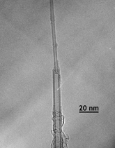
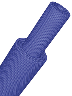
| The controlled and reversible telescopic extension of multi-walled carbon nanotubes, as shown [above right] in both the transmission electron microscope image and the computer graphic [above], could lead to virtually frictionless nanoscale linear bearings and constant-force nanosprings. | |
"What we are seeing is the world's smallest room temperature rectifier, one that is only a handful of atoms in size," Zettl said at the time of the discovery in the fall of 1997.
Another hot application anticipated for nanotubes is in the area of micro-electromechanical systems or MEMS. Development of MEMS has been hampered by frictional wear and tear that occurs in all devices made from silicon or silicon-based compounds. Last year, Zettl and members of his research group custom-engineered carbon MWNTs into seemingly frictionless bearings and switches that could prove immensely valuable to MEMS. Working with an STM inside a high-resolution transmission electron microscope, the researchers peeled off the outer layers of a carbon MWNT while leaving the core nanotube within fully intact and protruding. They then demonstrated this core nanotube could be made to slide in and out of its surrounding jacket like a well-oiled shaft moving in and out of its sleeve.
"Repeated extension and retraction of telescoping nanotube segments revealed no wear or fatigue on the atomic scale," said John Cumings, a graduate student in Zettl's group. "Hence, these nanotubes may constitute near perfect, wear-free surfaces."
The possibility of using telescoped nanotubes as really small and incredibly fast electromechanical switches arose when it was found that a fully extended core tube would snap back into its jacket in less than ten billionths of a second.
Explains Cumings, "Because the core nanotube conducts electrically to its housing, an extended core could bridge a gap between two metals, closing a circuit. When the core nanotube is retracted, it would open the circuit."
|
|
|
| Physicist Alex Zettl, shown here with a model of a carbon nanotube, has made ball bearings and mechanical switches far too small to be seen without the aid of an electron microscope. | |

Soon afterwards Zettl and his group, in collaboration with other groups outside of Berkeley, found that the electronic properties of carbon nanotubes are so extremely sensitive to oxygen that exposure to air can convert a semiconducting nanotube into a metallic conductor.
Working with SWNTs, the researchers studied both bulk samples and single isolated tubes, measuring electrical resistance and thermoelectric power, the voltage induced by a temperature gradient, under environmental conditions that gradually shifted from oxygen to vacuum and back to oxygen.
"The effects of oxygen exposure became increasingly more irreversible (and have longer time constants) with decreasing temperature, as expected for a gas adsorption process," Zettl says. "In fact, our transport measurements indicate that, once SWNTs have been exposed to oxygen, it is not possible to fully deoxygenate them at room temperature even under high vacuum conditions."
Nanotubes need not be made only from pure carbon. Any compound with a propensity for forming graphite-like sheets is potential nanotube material. Among the most intriguing of the noncarbon nanotubes are those made from boron nitride (BN), a compound with a uniform electronic bandgap independent of tube diameter or chirality. This electrical uniformity means that BN nanotubes can be doped to tune their conductivity much like silicon. The need has been for a reliable way to make large amounts BN nanotubes.
Zettl and his group have been able to meet this need through the use of an intensely hot electrical discharge between two boron-rich electrodes in a chamber filled with pure nitrogen gas. This plasma-arc method yields an abundance of double-walled BN nanotubes in the gray residue and soot that forms along the chamber walls. These double-walled nanotubes were found to self-assemble into nanotube bundles or ropes that can extend several hundred nanometers in length. Also to be found in the gray residue are BN-coated nanocrystals. Zettl and his group have discovered a means of hollowing out these crystals through chemical etching to create BN "nanococoons." Refilling these nanococoons with select atoms or molecules could hold important technological implications for the chemical and the electrochemical industries.
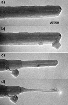 |
Transmission electron microscope images of a multiwall carbon nanotube being shaped. (a) A nanotube in its pristine form: it contains approximately 37 walls and has an outer radius of 12.6 nm. (b) A carbon onion has been inadvertently transferred to the nanotube end from the shaping electrode, but no attempt has been made to shape the nanotube. (c)(d) Results of the subsequent peeling and sharpening processes: the onion has simultaneously been displaced to a benign position down the tube axis. The shaped, or 'engineered', nanotube in (d) is thick and mechanically rigid along most of its length (not seen in the image), but tapers stepwise to a fine sharp tip that is electrically conducting and ideal for scanning probe microscopy or electron field emission applications. The final long nanotube segment contains three walls and has an outer radius of 2.1 nm. |
"With nanotubes, we're not seeing the beginning of something that might lead to something 25 years down the road," says Zettl. "These are things that are crying out to be exploited in the near future. Nanotubes are on a venture-capital timescale."
| < Research Review | Top ^ | Next > |