|
SCIENCE ON THE SURFACE
By LYNN YARRIS |
 |
|
SCIENCE ON THE SURFACE
By LYNN YARRIS |
 |
On December 29, 1959, the late Caltech physicist Richard Feynman presented a lecture at the annual meeting of the American Physical Society entitled, "There's Plenty of Room at the Bottom." In this talk, the Nobel laureate speculated as to what technologies might be achieved if scientists could fabricate devices on the scale of atoms and molecules. He offered up such notions as writing the Encyclopedia Britannica on the head of a pin using electron beam etching; building circuits with wires that are only a few atoms in diameter; and rearranging the atoms on the surface of a material in order to change its properties. It has been reported that some of Feynman's audience laughed-they thought he was joking.In 1991, the Office of Technology Assessment reported to Congress that the wave of miniaturization which swept over the electronics industry starting in the 1960s is on the verge of being supplanted by a second wave as we move into the 21st century. The first wave ushered in the age of microtechnology, which revolutionized the electronics industry and carved out computer markets worth well more than $100 billion annually. This second wave, the OTA report advised, will usher in devices with features a thousand times smaller than the microcircuits of today, and will most likely create entirely new technologies and open commercial arenas beyond computers that are potentially even more vast. What the OTA report was talking about and what Feynman so presciently predicted is the age of "nanotechnology," and it is rapidly coming upon us.
The word "nanotechnology" comes from nanometer, which means one billionth of a meter (about 25 millionths of an inch or 10 angstroms). Given that atoms range between one-tenth and one-half a nanometer in diameter, nanotechnology answers Feynman's call to work on an atomic-scale. Most of the nanostructures now envisioned would have dimensions of about 1 to 100 nanometers, making them roughly equivalent in size to a protein molecule. Nanotechnology advocates extol possibilities for engineering constructs so small they sound ripped from the pages of science-fiction novels. For example, the most outspoken of these apostles, scientific maverick and author Eric Drexler, has foretold of supercomputers that fit in the palm of the hand, molecular machines that fight disease and repair damage from inside the human body, and solar-powered nanofactories that patrol the atmosphere, scouring the air of pollutants. Though it reads like fiction, the scientific credibility is real enough for the U.S and Japanese governments to have begun a major push on nanotechnology research and development. Private industry is also weighing in with millions of investment dollars.
Proponents agree that the ultimate success of nanotechnology will hinge upon the ability of researchers to characterize and control the atomic structure of surfaces and interfaces. A solid material's chemical, electronic, and mechanical properties are largely determined by the atoms on its surface, or at the interface where two different solid surfaces meet. This is because the interior atoms of a solid are chemically bonded to neighboring atoms in all directions to form a bulk crystal. On the surface, however, neighboring atoms are missing in at least one direction, which leaves surface atoms more free to react or move around.
As the size of a material object shrinks to nanometer levels, the proportion of its atoms that are on the surface or at the interfaces also becomes much greater. There is talk now of future devices so small they become two or even one-dimensional objects-essentially nothing but surfaces and interfaces.
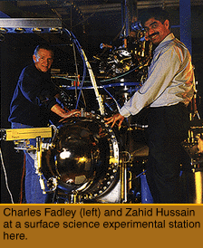
Two of the most powerful techniques known to researchers for studying solid surfaces are photoelectron spectroscopy and photoelectron diffraction-collectively known as PES/PED. One of the country's foremost practitioners of PES/PED is Charles Fadley, an Advanced Light Source professor of physics with a joint appointment at UC Davis and Berkeley Lab's Materials Sciences Division (MSD). For the past 25 years, Fadley has been making PES/PED measurements in laboratories and at major facilities all around the globe. Drawing from this deep well of experience, Fadley has overseen the installation of what is thought to be the most extensive surface science experimental station ever to be linked to the beamline of a synchrotron-radiation particle accelerator.
Electrically charged subatomic particles accelerated to speeds near that of light and then forced along a curved path give off light known as synchrotron radiation. Fadley's new PES/PED experimental station is located at Berkeley Lab's Advanced Light Source (ALS), an electron storage ring equipped with special magnetic devices that enable it to generate beams of x-ray and ultraviolet light at wavelengths and energies ideal for surface science studies.
In talking with Fadley, he will tell you that surfaces are both "wonderful and terrible" to study. The potential for bonding with other atoms that makes surfaces the key to chemical activity also creates great difficulty for researchers who would study them. In order to avoid problem-causing contamination from atoms in the surrounding environment, surfaces must be prepared with great care, usually under the difficult working conditions of ultrahigh vacuum.
"After the preparation," Fadley says, "special techniques also have to be used to avoid looking at the atoms in the bulk crystal. Most techniques that use photons to probe solid materials are bulk probes rather than surface probes, or have to be used in special geometries to enhance their surface sensitivity. The beauty of photoelectron spectroscopy and diffraction is that the only effects measured are those that come from within the first 5 to 10 layers of atoms in a material (the chemically active layers)."
Though the execution is tricky, the principle behind Fadley's research technique is relatively simple. It is based on the "photoelectric effect" which was first explained by Einstein at the turn of the century. It starts with a beam of photons striking the surface of a sample to be studied. Electrons in the first few layers of the sample's atoms absorb the incoming energy and are ejected from the sample as photoelectrons. In PES these photoelectrons are emitted at energies that can be measured to identify each type of emitting atom, and to determine how many there are and what their chemical or magnetic state is. But the principles of quantum theory also dictate that photoelectrons emitted from the inner shells of an atom must also be treated as outgoing spherical waves that can be scattered by nearby atoms. In PED, these scattered waves in turn produce diffraction patterns that can be analyzed to locate the positions of the atoms.
Fadley's experimental station has been constructed to capitalize on the high quality of light delivered by the ALS. In addition to its unique PES/PED system, the station also features state-of-the-art sample preparation and characterization equipment. To design and assemble it, Fadley worked closely with ALS scientist Zahid Hussain. Another collaborator was former Berkeley Lab Director David Shirley, who is now a dean at Penn State University. Graduate students and postdoctoral associates from both UC Davis and UC Berkeley also played key roles.
"It was no small feat to put together all the components we needed to construct this experimental station and have all of the components perform so well," Fadley says. "I don't think it would have been possible anywhere but at the ALS."
The ALS, which opened in the fall of 1993, is a so-called "third-generation" synchrotron radiation facility (the latest in the evolutionary line of synchrotron light sources) and the nation's premier source of "soft" (low energy) x-rays and ultraviolet light. The largest and most sophisticated accelerator ever constructed at Berkeley Lab, the ALS can boost the energy of electrons to about 1.5 billion electron volts (1.5 GeV) and orbit them for several hours around a storage ring in a tightly constrained, ribbon-shaped beam that is no thicker than a human hair. Beams of photons are extracted from this orbiting electron beam when it passes through one of three types of magnetic devices-dipole or "bending" magnets, which bend the path of the electrons so as to produce a sweeping, searchlight beam; and wigglers and undulators, which bend the path many times to produce brighter and more focused (almost laserlike) beams. The ALS was constructed with funding from the Materials Sciences Divison of the Office of Basic Energy Sciences at the Department of Energy. Berkeley Lab's Materials Sciences Division has also contributed significantly to the construction of five ALS beamlines.
 |
 |
 |