|
March 29, 2000 |
|
 |
 |
 |
||
|
|
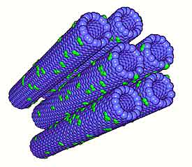
Surprising results from a new study on the
electronic properties of carbon nanotubes -- hollow cylinders of pure
carbon about 50,000 times more narrow than a human hair in diameter --
show that these amazing materials may be even more versatile than anyone
had previously thought.
As part of a broad program investigating the synthesis, characterization and theoretical modeling of carbon nanotubes, scientists with the U.S. Department of Energy's Lawrence Berkeley National Laboratory (Berkeley Lab) and the University of California at Berkeley have reported that the electronic properties of these tubes are so "extremely sensitive" to oxygen that exposure to air can convert a semiconducting nanotube into a metallic conductor.
"Many supposedly intrinsic properties measured on nanotubes may be severely compromised by extrinsic air exposure effects," the scientists state in a paper published in the March 10 issue of the journal Science. Some proponents of nanotubes may find this result discouraging, but not Alex Zettl, a physicist who holds a joint appointment with Berkeley Lab's Materials Sciences Division (MSD) and UC Berkeley's Physics Department and is one of the coauthors of the Science paper. "This is not a negative finding," he says. "Our results show that carbon nanotubes are far richer materials than we have appreciated. We can now envision even more applications in addition to those already proposed for them. We will need to apply relevant theories to explain our observations and we may need to reinterpret previous data, but I see entirely new doors opening for carbon nanotubes." The other coauthors of this study were Philip Collins, who is now with IBM's T. J. Watson Research Center in New York, and Keith Bradley and Masa Ishigami of UC Berkeley. Says Collins, "We've demonstrated that carbon nanotubes can behave as both n-type and p-type semiconductors. Until now, all nanotube measurements had suggested p-type conducting behavior only." In their paper, the Berkeley researchers found that the degree of oxygen exposure is the determining factor as to whether a carbon nanotube functions as an n-type or p-type semiconductor. The ability to function as either type is critical if nanotubes are to ever replace conventional silicon devices. Says Collins, "Junctions between these two types of semiconductors serve as the electronic building blocks for diodes and transistors. Without both types, the variety of electronic devices which could be built from nanotubes would be severely limited."
Zettl suggests that in principle, a nanotube's electronic properties could be controlled through the use of "protective coatings" to shield select portions of the nanotube from oxygen exposure. "It should be relatively simple to keep oxygen on or off specific areas of a nanotube," he says. Carbon nanotubes have been highly touted for their potential to succeed silicon in future electronic devices. Chemically inert and stronger than steel, nanotubes behave as if they are one-dimensional objects, hence not subject to the size and heat restrictions that will eventually limit silicon-based devices. Nanotubes also offer a full range of very useful intrinsic electrical and thermal conductivity properties. Prevailing theories have held that the electronic properties of a nanotube are dictated solely by the diameter and chirality (geometric configuration) of the tube. Theories also predicted that natural defects in the hexagonal web of a nanotube's carbon atoms (nanotubes are essentially tiny sheets of graphite that have been curled and connected along a seam like a drinking straw) would give rise to the creation of atomic-sized electronic devices, a prediction that experiments in 1997 by Zettl and Collins confirmed. In their latest study, Zettl and his associates found that the chemical environment surrounding a nanotube is at least as important an influence on the tube's electronic properties as its diameter. Working with single-walled carbon nanotubes (SWNTs) grown by conventional laser ablation methods, the researchers studied both bulk samples and single isolated tubes. Measurements of both electrical resistance and thermoelectric power, the voltage induced by a temperature gradient, were made under environmental conditions that gradually shifted from oxygen to vacuum and back to oxygen. "The effects of oxygen exposure became increasingly more irreversible (and have longer time constants) with decreasing temperature, as expected for a gas adsorption process," the scientists state in their Science paper. "In fact, our transport measurements indicate that, once SWNTs have been exposed to oxygen, it is not possible to fully deoxygenate them at room temperature even under high vacuum conditions." Further evidence that the effects being observed were the result of gas adsorption came when the topology of the nanotubes was changed. Dilute SWNT thin films yielded quick electronic changes, while optically thick films required higher temperatures and longer times to reach equilibrium. The experiments were repeated with different major gas constituents of air to confirm that the changes in electronic properties were due to oxygen adsorption. Carbon materials such as charcoal are known for their excellent adsorption and sieving properties, but nanotubes were thought to have been an exception because of their morphology, especially the smoothness of their exterior surface. In light of these new findings, the Berkeley researchers believe that carbon nanotubes could find valuable use as sensors for oxygen and other gases. In shifting their exposure environments from oxygen to vacuum and back to oxygen, the Berkeley researchers found that the TEP voltage sign switched from positive to negative and back to positive. A positive sign means the charge carrier is like an electron "hole" which for a seminconducting nanotube means a p-type semiconductor. A negative sign means the charge carrier is an electron, which for a semiconducting nanotube means an n-type semiconductor. What this suggests, say the Berkeley researchers, is that previous studies identifying carbon nanotubes as p-type semiconductors were the result of nanotubes having been "doped" with adsorbed oxygen. "It is important to keep in mind that all of the electronic properties which have been reported for nanotubes are still real," says Zettl. "The only question is to what extent did those results depend upon the presence of oxygen. I'm still very excited about the prospects for nanotubes as electronic devices." Zettl's group is one of several in the Materials Sciences Division (MSD) at Berkeley Lab that is studying various aspects of carbon nanotubes. Other principal investigators in this broad MSD effort include Marvin Cohen, Steven Louie, Rob Ritchie, Uli Dahmen, and Paul McEuen. In predicting and demonstrating the synthesis of novel forms of these tubes and characterizing their highly unusual mechanical and electronic properties, these investigators have shown that carbon nanotubes could serve in applications as diverse as exceptionally strong structural fibers or flat panel displays. Berkeley Lab is a U.S. Department of Energy national laboratory located in Berkeley, California. It conducts unclassified scientific research and is managed by the University of California. |