|
Spring 1993 |
|
 |
 |
 |
||
|
|
LBL scientists are using scanning tunneling
and atomic force microscopes to image the arrangement of atoms on
surfaces. In the future, these instruments may be used to manipulate
individual atoms.
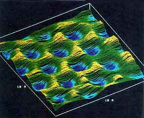
Miquel Salmeron learned about the development of the scanning tunneling microscope shortly after it was invented a decade ago. Gerd Binnig and Heinrich Rohrer of the IBM Research Laboratory in Switzerland had developed a new device capable of imaging and even manipulating details as small as a single atom. "Right away, those of us who are surface scientists knew this was a revolutionary breakthrough," recalls Salmeron, a researcher in LBL's Materials Sciences Division. "The characteristics of a material--its reactivity, its mechanical properties, its behavior in an electronic device--largely are determined by the atomic structure of its surface. "Researchers had been using all kinds of techniques for 20 years to determine the atomic structure of surfaces. None allowed us to see individual atoms, with the sole exception of the field ion microscope for imaging a few metals. Suddenly, the scanning tunneling microscope arrived. For the first time, we could see atoms on any conductive surface." By 1986, five years after its invention, the scanning tunneling microscope (STM) had become such a vital tool in materials science and chemistry that Binnig and Rohrer were awarded the Nobel Prize in Physics. The instrument creates images using a radically different means than conventional light or electron microscopes. It uses a sharp tip, almost like that of a phonograph stylus, and as it scans over an object, it maps out a three-dimensional image.
Salmeron began working with the STM in 1985. Today, he heads an LBL Center for Advanced Materials research program that has as its hub the STM and a related offspring instrument, the Atomic Force Microscope (AFM). Salmeron and collaborators Frank Ogletree, Joe Katz, and William Kolbe have developed unique versions of STM and AFM microscopes, along with advanced electronic controls and computer software. Several of these advances have found their way into commercial microscopes. At LBL, the STM and AFM are vital components of more than a dozen current research projects. The work includes the study of the surface structure of catalysts under reaction conditions, explorations of the feasibility of mapping and sequencing DNA, studies of the atomic-scale mechanical properties of lubricated surfaces, examinations of semiconductor interfaces, and the use of lasers to capture and image extremely fast, nanometer-scale interactions. A decade ago, the term nanometer (a billionth of a meter) was not common parlance in the high-technology community. By making nanometer-scale objects accessible, the STM and AFM are playing a major role in the ascendance of nanometer-scale science and technology. To understand how the two instruments actually work, one needs to discard the usual notion of a microscope. The STM and AFM do not create images the way a conventional microscope does. They rely on what might loosely be called touch. Indeed, one STM scientist, Carlos Bustamante of the University of Oregon, calls the instruments "a kind of Braille way of looking at molecules." The STM creates an image by scanning a tip across a sample. A computer records the precise location of the tip and generates an image based on the path of the tip as it moves above a sample at a constant height. The device owes its existence to a quantum mechanics effect in which an electron can penetrate an energy barrier. According to quantum mechanics, explains Salmeron, the wave function of an electron extends out beyond the surface of any material. The STM takes advantage of the overlap between the electron wave functions surrounding the object to be imaged and the wave functions of the electrons associated with the STM's tip. When the tip is moved to within a few angstroms of a sample's surface, a current of electrons crosses the gap--a phenomenon known as "tunneling." (The sample must be conductive or affixed to a conducting substrate.) Because tunneling is very sensitive to the distance between the tip and the sample, the STM can map out the surface of the sample with great precision. In one mode, researchers use an electrical feedback mechanism to maintain the tip at a constant distance as it scans over the sample, up and down over surface contours as slight as single atoms. Topographical data are recorded and translated into a three-dimensional image by a computer. The AFM, a descendant of the STM, does not require that the sample or substrate be conductive. The instruments are similar in that they both use a tip to sense the atomic shape of a sample as well as a computer to record the path of the tip and generate an image. However, the AFM tip "touches" the sample. In a phonograph needle, about one gram of force is applied on the stylus; in the AFM, the load on the tip is about one ten-millionth of a gram, a force so slight that it does not dislodge even a single atom. Translated into quantum mechanical terms, the electron wave functions of the tip and the sample being imaged can overlap strongly enough to give rise to strong repulsive forces. Thus, in the AFM, the tunneling current upon which the STM relies is replaced by the force between the tip and the sample. The instrument can be adapted to sense a range of forces, including attractive or repulsive, interatomic, electrostatic, and magnetic forces. These forces cause angstrom-size displacements of the cantilevered tip, movement which is recorded and translated into a topographic image. Though nanometer-scale engineering is a potential use of the STM and AFM, atomic-resolution imaging remains the current focus of the LBL program. "We are interested in studying surface problems like the atomic-scale mechanical properties of surfaces," says Salmeron. "Clearly, the information derived from these microscopy studies is providing new insights." Surfaces are critical in the performance and interaction of materials. To improve performance and to create new materials, scientists study surfaces, attempting to learn what happens at an atomic level. Until the advent of the STM and AFM, surface science took place in a vacuum. Literally. Explains Salmeron, "Surface science has relied on analytical techniques that only work under high vacuum conditions. Over the years, scientists have done these studies under vacuum and hoped they were still relevant to the real world. This has been a major impediment. "However, the STM and AFM don't require a vacuum. We are now imaging surface reactions under normal atmospheric pressures as well as at high pressures. The pressures can range from one to 100 atmospheres--whatever pressure and temperature are typically used for the reaction we are studying. We are the first in the world to do this." In collaboration with Gabor Somorjai, who heads LBL's Surface Science and Catalysis Program, and UC Berkeley graduate student Brian McIntyre, the researchers are using the new high-pressure STM techniques to study platinum, the most versatile and common catalyst. Platinum, for instance, is used in catalytic converters in automobiles to reduce exhaust emissions. Nobody has ever seen the atomic arrangement of a platinum surface as it catalyzes reactions in the exhaust gas. Scientists know that surface reactions can be almost cataclysmic, like an earthquake warping the entire surface. And they know that platinum makes the reaction go. But they don't know exactly why or how it works. Observing each step in the reaction might very well allow scientists to alter and improve the reaction.
So far, LBL researchers have examined the platinum surface under reaction pressures before and after the adsorption of carbon monoxide, hydrogen, oxygen, and sulfur. Under atomic-resolution magnification, they have been able to observe changes in the atomic structure due to the reaction conditions. "Chemical reactions often happen on the irregularities, the defects of a surface," explains Salmeron. "Chemical activity is greatest where atoms of platinum are missing or at steps in the material. We are looking for these magical places where the reaction proceeds. "Already, we have observed the migration and diffusion of sulfur on the surface. Ultimately, we want to see the reaction as it proceeds at the atomic scale. We want to look at a long list of catalysts and trace the fate of individual atoms throughout the course of the reaction." The epitaxial or layered growth of materials is another field of chemistry that is under investigation with the new microscopes. LBL researchers are examining the growth of metal oxides on catalysts--for example, the growth of titanium oxide and iron oxide on platinum--and studying how islands of these metal oxides modify the catalytic properties of platinum. Because titanium oxide and iron oxide are not by themselves catalysts, this effect is not understood. Through microscopic images, the researchers have viewed islands made of a few atoms of these oxides and noted that titanium atoms at the perimeters of these patches have higher tunneling probability, apparently because they are less oxidized than atoms at the center. This observation suggests that the edges of these metal oxide islands may be responsible for the enhancement of certain catalytic reactions. In the field of electronics, Salmeron's group is investigating how to improve gallium arsenide semiconductors in a collaboration with Eicke Weber, an LBL researcher and professor in UC Berkeley's Materials Science and Mineral Engineering Department, and graduate student Jun Fei Zheng. To accomplish this, they are using an STM with a tip that can be navigated. Rather than beginning its mapping of the atomic landscape at a random point, the "Johnny Walker" STM (so named because it can walk around) can be steered to the interfaces between different semiconductors or metals. "These interfaces are critical in microprocessors," says Salmeron. "You have to have a clean flow of electrons. Different semiconductor materials have different electronic properties, which depend upon their atomic structure. We want to know if there are more defects, more missing or excess atoms, as you approach the interface. "Now, we can see exactly what defects have been introduced by different aspects of the fabrication process. Chemical treatments, the type of metal contacts, the effect of the heat used to create interfaces on the nearby current carriers in the semiconductor -- all these processes can alter electron flows. We hope to be able to identify which processes create adverse changes and which create the most favorable interfaces." Just as with a light microscope, researchers can vary the level of magnification of an STM or AFM image. The tips of both instruments scan across a sample, propelled by a piezoelectric driver which mechanically moves the tip when it is stimulated by an electric signal. The more voltage, the greater the movement of the tip, and the larger the area being imaged. One-tenth of a volt, for instance, moves a tip about one angstrom or the width of a single atom. Ogletree says that for scientists seeking to observe what is happening at an atomic scale, the STM and AFM provide "instant gratification." Snapshots of a surface can be created in one to two seconds. Imaging with the STM and AFM is similar to conventional photography in terms of the effects of long exposures. The faster the image is created, the less likely the subject will move and cause the image to be blurred. In the case of the microscopes, surface temperature differences affect the motion of the tip. The longer the tip takes to scan a sample, the greater the distortion. Several seconds can elapse during the creation of an image without thermal distortion occurring. Through a succession of images, scientists can even observe atomic-scale events evolving on a surface. However, the microscopes have not been nearly fast enough to record intermediate reactions, events that occur on a lightning-like, picosecond (trillionth of a second) timeframe. Through the use of lasers, the scientists hope to be able to witness intermediate reactions. Currently, pairs of lasers are in common use as tools to measure the dynamics of surface reactions. After a pump laser stimulates a surface, a probe laser is used to measure the event. In collaboration with LBL Materials Sciences Division Director Daniel Chemla's group, the researchers are working on a process called time-resolved imaging, in which lasers are paired with the STM and AFM. "The general concept is to use one laser to modify a surface and a second, short-pulsed laser as a switch that turns the STM on and off in picoseconds," explains Ogletree. "While turned on, the STM is poised over a single point and stays there for a number of cycles to make sure its measurement is accurate. This process would be repeated over every point in a grid that is under examination. The result should be an atomic-resolution image of an intermediate stage that has a lifespan measured in picoseconds." Ogletree says one planned experiment would start with an undoped semiconductor--one without added impurities. Thus, the semiconductor would be without current carriers. Pulses of laser light would be used to create very short-lived carriers. "The precise progress of a pulse of electrons across a semiconductor is really an unknown," says Ogletree. "The velocity of these current carriers is about one angstrom per femtosecond (a millionth of a billionth of a second). With time-resolved imaging, we believe we can observe how an electron makes its way across a semiconductor. We can see how the pulse of electrons spreads as it moves and just how." Recently, the AFM has begun to make advances into another realm of science, that of biology. Back in 1987, Salmeron's group used the STM to create the first images ever produced of native DNA. These images showing the double helix suggested that the STM might be used in the Human Genome Project, which aims to map and sequence human DNA. Reproducing those first images of DNA, however, has proved to be a challenge. The STM requires either a conductive sample or a sample anchored to a conductive substrate. DNA is not conductive, and binding it to the substrate again has proved to be difficult. When the tip approaches a piece of DNA, the strong current exerted seems to dislodge the sample and push it aside. Salmeron says one way to keep the sample from slipping away is to raise the STM tip further above the sample. The downside to this approach is that it lowers the current level and lengthens imaging time to a blurry six minutes. Researchers have turned to the AFM, an instrument ideally suited to imaging nonconductive samples, and have now mastered the technique of imaging DNA with it. UC Berkeley biophysics graduate student Matthew Murray can image DNA routinely but, so far, not at a resolution where individual nucleotides can be discriminated. The LBL team has become the first to demonstrate that DNA labeled with proteins can be imaged with the AFM. Segments composed of 353 and 701 base pairs of nucleotides have been marked with a protein and imaged. Murray says this demonstrates that the AFM can be used to measure the distance between two points of DNA and to map DNA--that is, determine the chromosomal location of specific genes. Murray points out two important advantages to using the AFM for mapping. Compared to alternative techniques, such as gel electrophoresis, very little DNA is required, and the AFM is faster, producing an image in one minute as opposed to one hour. Could the AFM ever be used to reveal the sequence of the three billion nucleotides that compose the human genome? Several obstacles stand in the way. Segments of DNA that consist of less than 1000 pairs of nucleotides are relatively straight. But longer strands bind up into a tangled pile, much like snarled fishing line. Tangled DNA cannot be measured nor can the interior realm of the tangle be imaged. On the other hand, the distance between one nucleotide and another is about three angstroms, and the AFM can image details as small as one angstrom. Murray says that if a method can be devised to prevent longer strands of DNA from tangling, biologists will want to reassess the feasibility of using the AFM for sequencing. Rohrer, the co-inventor of the STM, has suggested that the "M" in STM and AFM really should be changed. Instead of microscope, he says, the "M" ought to stand for method. The instruments actually represent new methods for working on the nanometer scale. "By work," he wrote, "I mean observing a single, individually selected nano-object, measuring and understanding its properties, manipulating it, modifying it, and ultimately observing and controlling its possible functions and related processes." Salmeron recalls a widely publicized experiment that demonstrates some of the possibilities suggested by Rohrer. One year ago, IBM scientists used individual atoms of xenon to spell out the IBM logo. While clever, this was no idle stunt. Says Salmeron: "Many scientists are researching how to use the devices to make holes or mounds in substrates, creating a surface that can store digital information. Each hole or mound is the size of several atoms. "Think about the amount of information you could store with these devices. Say each letter requires a space the size of 10 atoms, or 100 angstroms. You could put one trillion letters in a square centimeter. That amounts to over one million books, each with hundreds of pages." Miniaturization has been a constant force in the march of technology, and Salmeron is convinced that the bounds of progress will be further broadened by the STM and AFM. "There is no technological impediment to mechanizing the STM and AFM, to using the instruments as computer-driven robots for atomic manipulation. The tips can be used as atomic scalpels. You can literally move around individual atoms. Like many scientists," says Salmeron, "I believe that one day we will do atomic engineering with these devices." -- Jeffery Kahn |