| January, 2007 | science@berkeley lab | | lab a-z index | lab home |
|
|||
| Zigzag Graphene Nanoribbons: A New Path to Spintronics | ||||||||||||||||||||
| Contact: Lynn Yarris, lcyarris@lbl.gov | ||||||||||||||||||||
Spintronics — the principle behind electronic devices based on the spin of an electron, in addition to its charge — is the gleam in the collective eyes of the computer industry. With the discovery by Berkeley Lab scientists of a new pathway towards realizing the spintronics dream, that gleam should light up even brighter.
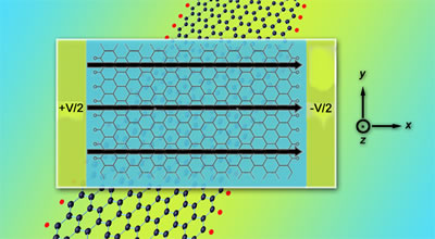
Marvin Cohen and Steven Louie, theorists who hold joint appointments with Berkeley Lab's Materials Sciences Division and the University of California at Berkeley, together with postdoctoral researcher Young-Woo Son, have calculated that nanoribbons of graphene — single-layered sheets of hexagonally-arranged carbon atoms — with zigzag edges can be made to carry a spin current. Zigzag graphene nanoribbons could therefore serve as the basis for nanosized spintronic devices. "Our calculations show that zigzag graphene nanoribbons are magnetic and can carry a spin current in the presence of a sufficiently large electric field," says Cohen. "An applied transverse electric field transforms the ribbon from a semiconductor with a small gap to a metal with carriers that are 100-percent spin polarized. By carefully controlling the electric field, it should be possible to generate, manipulate, and detect electron spins and spin currents in spintronics applications." Louie says, "There are, of course, many challenges to confront before this concept can be used for applications. However, if electric fields can be made to produce and manipulate a 100-percent spin-polarized carrier system through a chosen geometric structure, it will revolutionize spintronics technology." Spintronic devices promise to be smaller, faster, and far more versatile than today's devices. Spin is a quantum mechanical property that arises when the intrinsic rotational momentum of a particle, in this case an electron, creates a tiny magnetic field. For the sake of simplicity, spin is given the direction of either "up" or "down." The up or down values of spin can be used to encode data in the 0s and 1s of the binary system, just like the positive or negative values of an electrical charge. However, unlike charge-based data storage, spin-based data storage does not disappear when the electric current stops. One of the keys to the future development of spintronic technology is the curious, extremely rare class of materials known as "half metals." These materials are unique because their conducting electrons are all spin-polarized in either the up or down orientation. Conduction takes place by charge carriers exclusively oriented in a single spin direction; the spin polarization of the carriers in half metals is theoretically 100 percent, making them ideal for spintronic device structures. The search for half metals among semiconductors has been intense, but to date there have been few investigations into organic materials, even though carbon-based nanostructures hold significant promise for future electronic devices. Says Louie, "Although there are organic magnets in molecular and polymeric forms, carbon in the crystalline form is not magnetic. This is probably the reason why people haven't been looking for half metals in carbon-based nanostructures such as graphene."
Using first-principles calculations, which can predict a material's electrical and magnetic properties from the atomic number and mass of its constituent atoms, plus the brute computational power of the Department of Energy's National Energy Research Scientific Computing Center (NERSC), Cohen, Louie, and Son were able to demonstrate the half-metallic phenomenon in graphene nanoribbons. They showed that the half-metallic property emerges when homogeneous electric fields are applied across graphene nanoribbons whose zigzag-shaped edges are attached to voltage contacts. Zigzag edges form when the carbon chemical bonds of a honeycombed sheet of graphene are uniformly cut. "The electric fields can be used to directly manipulate the spin orientation of carriers in zigzag graphene nanoribbons by shifting the energy of different magnetic states via the electric field," says Louie. "We believe this is the first demonstration of such an effect." Cohen says, "It's very hard to polarize spins and even harder to manipulate them. Usually one needs magnetic fields that involve large pieces of equipment, which makes the production of small devices difficult. Here we get to have our cake and eat it too, because it is the electric field rather than the magnetic field that gives us the highest degree of polarization." Basing spin polarization on electric fields makes it much easier to work with small devices. "Also, the zigzag graphene nanoribbons are resistant to heat build-up, relatively insensitive to temperature, and are nontoxic," says Cohen. "All we need now is for clever nanoscientists to use our first principles calculations to design and make these or similar systems." This research was supported by the National Science Foundation (NSF) and by the Director, Office of Science, Office of Basic Energy Science, Division of Material Sciences and Engineering of the U.S. Department of Energy. Additional information
|
||||||||||||||||||||
| Top | ||||||||||||||||||||