| October 26, 2006 | science@berkeley lab | | lab a-z index | lab home |
|
|||
| Breaking Down the Barriers to Carbon-based Electronics | ||||||||||||||||||||
| Contact: Lynn Yarris, lcyarris@lbl.gov | ||||||||||||||||||||
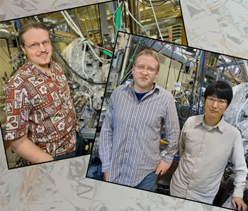
It's easy to see why the world's electronics industry covets the development of carbon-based devices. Carbon-based materials can act as superconductors and can emit light, something silicon can't do. Carbon-based materials are also especially promising as elements of nanometer-scale devices, high in efficiency and low in power consumption. Because of technical obstacles hampering their development, carbon-based materials have long been an elusive pot of gold at the end of the rainbow. After a decade of work, however, the technical barriers are beginning to be torn down, as evidenced by results from a recent experiment at Lawrence Berkeley National Laboratory's Advanced Light Source (ALS). Led by ALS scientist Eli Rotenberg, an international collaboration of researchers has demonstrated the potential of using bilayer graphene as a switching device in nanoscale electronic devices.
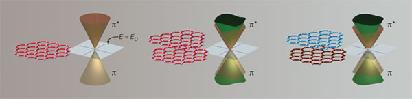
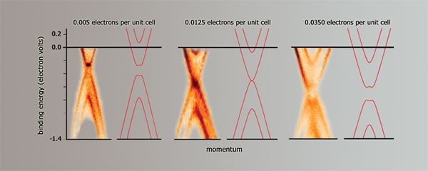
Graphene is a single layer of hexagonally-arranged carbon atoms forming a two-dimensional sheet, which can serve as the basic "mother system" of many carbon-based materials. For example, roll the sheet into a cylinder, seal the seam, and you have a carbon nanotube. Graphene has enormous potential for use in ultrafast electronic transistors, if an effective means of controlling the transport of electrical charge carriers (electrons or holes) through the sheet can be developed. This will require electronic bandgap engineering, the ability to alter the energy levels separating graphene's valence and conduction bands. These are the energies where electrons are tightly bound to their host atoms (valence band) or where electrons are free to move through a material (conduction band). While bandgap engineering is the basis of our semiconductor technology, it has not been applied to graphene — until now. Using a probe technique called ARPES (angle-resolved photoemission spectroscopy), plus the unique research capabilities of ALS beamline 7.0.1 — also known as the Electronic Structure Factory — Rotenberg and his collaborators characterized the electronic band structure of a bilayer of graphene thin films deposited on a substrate of insulating silicon carbide. Creating an asymmetry between the two layers by doping one sheet with adsorbed potassium atoms enabled Rotenberg and his colleagues to control the gap between the valence and conduction bands.
"This control over the band structure suggests the potential application of bilayer graphene to switching functions in electronic devices with a thickness of only two atomic layers," said Rotenberg. "We chose potassium doping as a means of achieving this, but the switching functionality could also be readily induced by an electric field across the bilayer in a device structure." Rotenberg and his colleagues, Taisuke Ohta and Aaron Bostwick of Berkeley Lab, Thomas Seyller of Erlangen-Nurnberg University, and Karsten Horn of the Fritz Haber Institute in Germany, reported the results of their experiments in a recent issue of the journal Science. "We were surprised at how high the current capacity was," Rotenberg said. "At a temperature of 30 Kelvin, which is cold enough to preclude any conduction through the substrate, we were able to pass 400 milliamps through a macroscopic sample. This corresponded to a current of about 20 million amps per square centimeter, which is the same order of magnitude reported for single-walled carbon nanotubes and graphene multilayers." If undoped, a bilayer of graphene sheets is considered a semimetal, a material in which the conduction and valence bands slightly overlap in energy. When Rotenberg and his colleagues first synthesized their bilayer graphene films onto the silicon carbide substrate, the graphene became a weak n-type semiconductor, having an excess of negatively charged electrons; the interface layer acquired an excess of conduction electrons from the substrate, creating a small bandgap. Potassium atoms deposited onto the graphene donated their lone valence electrons to the graphene's surface layer, and initially this resulted in closing the bandgap. But as the potassium deposition continued, the bandgap was reopened by the excess of electron charge-carriers on the graphene's surface layer. Progressive potassium deposition further enhanced the n-type doping.
"We could only achieve a limited degree of n-doping in the graphene with our technique," said Rotenberg. "Making a real switching device will require a more sophisticated doping of the graphene bilayer so that the energy gap controlled by an applied electrical field coincides with the energy of the least-bound electrons, the Fermi energy." The Electronic Structure Factory (ESF), which is managed by Rotenberg, utilizes a state-of-the-art undulator magnet to generate beams of x-rays with properties similar to that of a laser. These coherent and tunable x-ray beams are a hundred million times brighter than those from the best x-ray tubes and provide an exceptionally high degree of angular resolution for ARPES experiments. Rotenberg and his colleagues at the ESF are now designing a new ARPES instrument that will enable them to examine patterned graphene devices where they hope to control the doping by applied electrical fields. "This will allow us to introduce doping without the introduction of additional defects in our samples, so we can see the intrinsic changes that limit the lifetimes of electron charge carriers," Rotenberg said. "We will also be able to carry out measurements on related materials, such as single-wall carbon nanotubes, and follow how the electron structure and dynamics evolve as the nanotubes are decorated with foreign atoms and molecules. This has applications in nanoscale electronics as well as chemical sensors." Additional information
|
||||||||||||||||||||
| Top | ||||||||||||||||||||