| March 31, 2006 | science@berkeley lab | | lab a-z index | lab home |
|
|||
| Probing Organic Transistors with Infrared Beams | ||||||||||||||||||||
| Contact: Lynn Yarris, lcyarris@lbl.gov | ||||||||||||||||||||
Beams of extremely bright, tightly focused infrared (IR) light generated at Berkeley Lab's Advanced Light Source (ALS) have been used to directly probe the electronic properties of nanometer-scale field-effect transistors made from organic polymers. The results of this unique study could help the future development of sensors, displays, and plastic electronic components for cell phones, wireless internet devices, and other mobile electronic equipment.
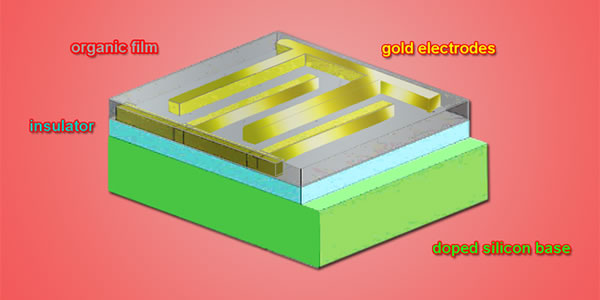
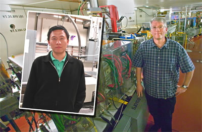
Field-effect transistors, or FETs, are used to amplify wireless and other weak electromagnetic signals. While silicon-based FETs have become ubiquitous in wireless technology, there is a growing push for the development of organic FETs for optoelectronic products like the large-area displays used in flat-screen TVs and computer monitors. "We have succeeded in probing the electronic excitations in organic FET devices only a nanometer thick, using infrared spectromicroscopy," says Zhiqiang Li, an ALS Doctoral Fellow from the University of California at San Diego. (A nanometer is a billionth of a meter, ten thousand times thinner than a human hair.) "Our results show that IR spectromicroscopy is well suited for the study of organic FETs and can provide information that is difficult, if not impossible, to obtain from other experimental techniques." Li adds that "organic FETs are already employed in the displays of mobile electronic appliances such as cell phones, but they have a potentially much bigger future in large-area displays, which demand a lightweight and structurally flexible material — as well as in chemical and biological sensors, molecular electronics, organic spintronics, and radio-frequency identification tags. Organic FETs are also offer the advantage of being easy to mass-produce at a very low cost." But the development of organic FETs has been hampered by a poor understanding of electronic processes in these materials. The ability of a FET to amplify an electromagnetic signal depends upon the density of the charge carriers (electrons or holes) that can be introduced into its conducting channel. In an organic FET, the conducting channel resides in a nanometer-thick layer at the interface of the device's semiconducting and insulating layers; here, high-density charges can result in the formation of polarons, distortions in the crystal lattice that create energy wells. An energy well can trap an electron much like a divot on a fairway can trap a golf ball, and this can impede the flow of charge-carriers, which in turn can impede the performance of the FET. "An experimental novelty of our work is that we have been able to employ infrared light to directly probe high-density charges in a functional organic FET device without the need for metallic contacts that could interfere with the intrinsic properties of the active organic semiconductor," says Li. "Because of the nanometer scale of the organic FET channels, some of the most informative spectroscopic probes in the arsenal of science, including scanning tunneling microscopy, photoemission spectroscopy, and neutron or inelastic x-ray scattering, are ruled out. As an inherently contactless probe, IR spectromicroscopy allows us to explore the landscape of charges in the conducting channel with a high degree of spatial resolution." The Right Tool for the JobThe application of IR spectromicroscopy to nanoscale FET materials was made possible by the exceptionally high brightness and focal spot size of the infrared beams at the Advanced Light Source. The ALS is an electron synchrotron designed to accelerate electrons to energies of nearly 2 billion electron volts (2 GeV), focus them into a tight beam, and send this beam around the curved path of a storage ring for hours at a time. Light can be extracted from the stored electron beam through the use of special magnetic devices. While the ALS is optimized for the production of x-ray and ultraviolet light, it also generates intense beams of photons in the IR, or terahertz, spectrum.
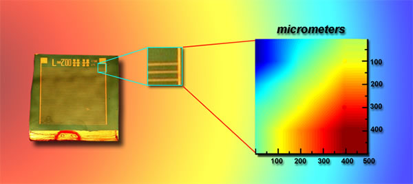
Michael Martin, one of Li's collaborators in this study, is the manager of ALS beamline 1.4.3, a bend-magnet beamline using light at wavelengths ranging from 1 to 20 microns. By using beamline 1.4.3, Martin and Li and their collaborators were able to acquire infrared spectra from individual spots on samples that measured less than 10 microns (10 millionths of a meter) in diameter. In addition, an automated mapping stage at the beamline was used to scan the samples under the beam and create infrared images. "For the organic FET samples we could obtain infrared spectral images while the FET had a bias voltage applied, then use the changes in the infrared spectra to map out exactly how many charge carriers were in the sample," Martin explains. "We also used the high-resolution imaging capability of beamline 1.4.3 to directly measure how far away from the voltage lead the charge-carriers are injected into the FET." Results of the first use of ALS beamline 1.4.3 for the study of organic FETs appeared in the journal Nano Letters in a letter titled "Infrared Imaging of the Nanometer-Thick Accumulation Layer in Organic Field-Effect Transistors." Li and Martin coauthored the paper with Guangming Wang, Daniel Moses, and Alan Heeger of UC Santa Barbara, and Na Sai, Massimiliano Di Ventra, and Dimitri Basov at UC San Diego. In their paper, the authors report the application of IR spectromicroscopy to study the injection of high-density charge carriers into bottom-contact FET devices based on a thin film of poly(3-hexylthiophene), or P3HT. This semiconducting polymer features exceptionally high charge-carrier mobility. Comparisons were made between P3HT devices deploying insulating layers of either silica or titanium dioxide, an insulator with a high dielectric constant. Insulators with a high dielectric constant are much desired in FETs because they allow for a much higher density of charge carriers in their channels than silicon-based FETs.
"Our measurements revealed severe restrictions of the channel length in devices based on high-dielectric insulators, which is particularly important if you want to use these insulators in chemical or biological sensors," says Li. "The search for high-dielectric insulators to replace silicon-based FET technology is currently the subject of a worldwide research effort. With our IR spectromicroscopy technique, we've shown that we can critically evaluate the merits and pitfalls of high-dielectric-constant materials in organic FETs, a capability that should be very useful in the search of optimized high-dielectric organic FETs." Additional information
|
||||||||||||||||||||
| Top | ||||||||||||||||||||