| BERKELEY, CA — The urgent search
for more efficient solar cells has recently focused on incorporating small amounts of
nitrogen into the semiconductor alloy gallium indium arsenide. Nitrogen atoms have a small
ionic radius; usually, the incorporation of smaller atoms into a semiconductor alloy
causes the material's band gap to increase. In striking contrast, adding even a little
nitrogen to gallium indium arsenide decreases its band gap dramatically, an effect of
great significance for the design of advanced solar cells. This surprising behavior has
now been explained by scientists at the Department of Energy's Lawrence Berkeley National
Laboratory, working with colleagues at the National Renewable Energy Laboratory (NREL).
The researchers found that nitrogen forms a narrow energy band in gallium indium arsenide
that splits the alloy's conduction band in two. The subbands push each other apart, and
the lower subband reduces the fundamental band gap.
 |
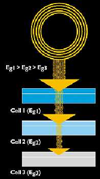
 A MULTIJUNCTION SOLAR CELL IS A STACK OF
INDIVIDUAL CELLS IN DESCENDING ORDER OF BAND GAP (EG). THE TOP CELL CAPTURES HIGH-ENERGY
PHOTONS AND PASSES ON THE REST, TO BE ABSORBED BY LOWER-BAND-GAP CELLS.
|
This discovery by the Berkeley Lab-NREL collaboration, which is sponsored by the
Photovoltaic Materials Project of the Department of Energy's Center for Excellence in
Synthesis and Processing, is of fundamental significance to the understanding of
semiconductor alloys and may suggest new approaches to the fabrication of highly efficient
solar cells.
"One reason today's solar cells are not very efficient is that no one material can
respond to a wide range of frequencies of sunlight," says Wladek Walukiewicz of
Berkeley Lab's Materials Sciences Division (MSD). "At NREL they invented a cell made
from thin layers of different alloys, with different band gaps sensitive to different
photon energies in the solar spectrum."
The band gap is the difference in energy between a semiconductor's valence band, which
is filled with electrons, and its conduction band, which is empty. (Bands are not physical
locations but energy levels, analogous to the energy levels of electron orbitals around an
atomic nucleus.) Since charge cannot flow in a completely full band or a completely empty
one, pure semi-conductors are usually insulators at low temperatures. Solar cells,
however, are designed so that when photons with enough energy boost electrons out of the
valence band into the conduction band, charge can flow in both bands— as negatively
charged electrons in the conduction band, or as positively charged "holes" in
the valence band.
 |
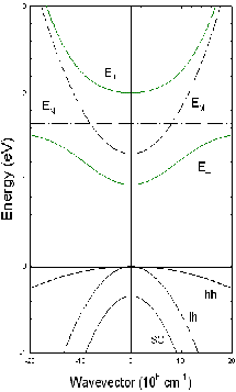
 THE CONDUCTION BAND (ABOVE) IN GALLIUM
INDIUM ARSENIDE IS SPLIT BY A NARROW ENERGY BAND FORMED WHEN A SMALL AMOUNT OF NITROGEN IS
ADDED TO THE ALLOY. THE LOWER SUBBAND REDUCES THE FUNDAMENTAL BAND GAP.
|
By depositing thin layers of gallium indium phosphide with a band gap of 1.8 electron
volts (eV) on layers of gallium arsenide with a band gap of 1.4 eV, NREL investigators
created a tandem solar cell with proven 30-percent efficiency— compared to
efficiencies of 10 to 16 percent typical of silicon. While too expensive for routine use,
the tandem cell has found a market in solar panels for communications satellites and other
spacecraft.
NREL researchers now want to add a third semiconductor layer to the cell, with an even
lower band gap responsive to lower energy photons in sunlight. They estimate that a layer
with a 1-eV band gap could increase such a cell's efficiency to 40 percent.
"They need a new material with a one-eV band gap and a crystal lattice structure
that matches that of gallium arsenide, so the layers can be grown next to each
other," says Walukiewicz. "They found that by adding just a little nitrogen to
gallium indium arsenide, they could achieve the desired band gap and an almost perfect
lattice match."
When nitrogen and other atoms with small ionic radii are added to most semiconductor
alloys, the band gap increases. Why should adding just a little nitrogen significantly
reduce the bandgap of gallium indium arsenide? Walukiewicz and his MSD colleagues Wei
Shan, Joel Ager, and Eugene Haller set out to solve the mystery.
Data from other semiconductors with low concentrations of nitrogen had indicated that
nitrogen produces "a localized, narrow band of its own," Walukiewicz says.
"Because nitrogen is so different from arsenic and the other elements in these
alloys, it doesn't mix — it keeps its own identity." The researchers calculated
that in gallium indium arsenide, this nitrogen band should lie a few tenths of an electron
volt above the lowest energy of the conduction band.
They predicted that the presence of the nitrogen level would split the conduction band
in two. "The nitrogen band is like a knife, it cuts the conduction band in
half," Walukiewicz says. Thus, while the band gap to the conduction band's lower part
was reduced to 1 eV, "there is also an upper conduction band, and we needed to find
it and characterize its behavior to prove our model."
On a substrate of gallium arsenide the researchers grew samples of gallium indium
arsenide with varying small concentrations of nitrogen. The samples, only 200 micrometers
(millionths of a meter) square and less than five micrometers thick, were examined with
modulated beams of light as the samples were squeezed in a diamond anvil cell to many
thousands of times atmospheric pressure.
Different colors of modulated light revealed the unmistakable signature of two
conduction bands; in agreement with Walukiewicz's model, the conduction bands initially
moved closer and then grew farther apart as the pressure was gradually increased. The
unequivocal observation of this repulsive "anticrossing," a well-known quantum
mechanical effect, confirmed the model.
The model also explains why, despite the small band gap, gallium indium arsenide with
nitrogen has so far proved disappointing in solar cells.
"The flat curvature of the lower band is not good news for electron
mobility," says Walukiewicz. As charge carriers, the electrons are short-lived and
tend to recombine with holes before they have traveled far enough to contribute to the
solar cell's output of electric current. "We are now working to see if the split-band
structure affects carrier mobility in a basic way, or if there are approaches that might
improve the situation."
One approach might be to increase the amount of nitrogen to as much as ten percent of
the alloy, through ion-beam implantation — although "atomic nitrogen is hard to
get, because nitrogen likes to be a molecule — it's the strongest-bound molecule in
the universe."
Another approach might be to substitute different small-ionic-radius atoms, such as
boron, for nitrogen. "But boron doesn't like to go into the alloy, and brute force
implantation could damage the semiconductor crystal."
It might also be possible to improve the quality of the alloy through novel growth
techniques, or through annealing or some other process that might reduce the number of
crystal defects which can trap and recombine charges. "After all," says
Walukiewicz, "even gallium arsenide was a lousy material with poor properties, in the
beginning."
Meanwhile, gallium indium arsenide with nitrogen holds promise for other applications
besides solar cells, such as in fiber optics, detectors, and light-emitting diodes. The
theoretical and observational studies of its completely new conduction-band structure open
a new perspective on the properties, behavior, and possible applications of other
"highly mismatched" alloys as well.
Wei Shan, Wladek Walukiewicz, and Joel Ager of Berkeley Lab's MSD, Eugene Haller of MSD
and the University of California at Berkeley, and John Geisz, Daniel Friedman, Jerry
Olson, and Sarah Kurtz of NREL report their findings in Physical Review Letters, 8
February 1999.
The Berkeley Lab is a U.S. Department of Energy national laboratory located in
Berkeley, California. It conducts unclassified scientific research and is managed by the
University of California. |

