| July 5, 2001 |
|
 |
 |
 |
||
|
|
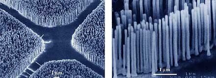
One of the smallest lasers ever made -- far too small to be seen even with the aid of the most powerful optical microscope -- has been successfully tested by a team of researchers with Lawrence Berkeley National Laboratory (Berkeley Lab) and the University of California at Berkeley. This device, which emits flashes of ultraviolet light, is called a "nanowire nanolaser" and it measures just under 100 nanometers in diameter or about one ten-millionth of an inch The nanowire nanolasers are pure crystals of zinc oxide that grow vertically in aligned arrays like the bristles on a brush. These crystal wire "bristles" range from two to 10 microns in length, depending upon how long the growth process was allowed to proceed. By comparison, the tiniest solid-state lasers in use today are fashioned from thin films of either gallium arsenide or gallium nitride and generally run several microns thick, or about one hundred thousandths of an inch. A typical human hair is about 100 microns thick.
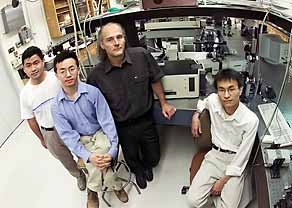
UNDER AN ELECTRON MICROSCOPE, THE ARRAYS OF NANOWIRE NANOLASERS LOOK LIKE BRISTLES OF A BRUSH, EACH BRISTLE AN INDIVIDUAL LASER ABOUT ONE THOUSANDTH THE DIAMETER OF A HUMAN HAIR.Photo by Peidong Yang/UC Berkeley, courtesy of Science "The ability to produce high-density arrays of light-emitting nanowires would open up lots of possible applications that today's gallium arsenide devices can't do," says Peidong Yang, a chemist with Berkeley Lab’s Materials Sciences Division and a professor with UC Berkeley’s Chemistry Department who was the lead scientist on this project. Collaborating with Yang from Berkeley Lab were Henning Feick and Eicke Weber, also with the Materials Sciences Division, and Samuel Mao and Rick Russo of the Energy and Environmental Technologies Division. Joining them were Michael Huang, Haoquan Yan, Yiying Wu and Hannes Kind, with the UC Berkeley Chemistry Department. A paper reporting this work appeared in the June 8 issue of the journal Science. To produce these nanowires, the research team used a standard crystal-growing technique called epitaxy in which one crystalline material is grown over the surface of another. In this case, sapphire crystals, coated in patterns with a thin film of gold, were plunged into a hot gas of zinc oxide. The gold film served as a catalyst and within ten minutes, millions of zinc oxide nanowires formed over the patterns on the sapphires.
Stated the authors in their Science paper, "This capability of patterned nanowire growth allows us fabricate nanoscale light emitters on a substrate in a controllable fashion." To produce light, the researchers used a process called "optical pumping." Working at room temperatures, the zinc oxide nanowires were flashed with light from a visible light laser. This light excited the zinc oxide molecules, causing them to emit photons. Cross-sections of the wires show them to be hexagonal and capped on the end. This cap is perfectly flat as is the interface between the wire and the sapphire substrate. These two perfectly flat surfaces act like mirrors and cause the photons emitted by the excited zinc oxide molecules to bounce back and forth between them. This reflected light causes the zinc oxide molecules to emit even more photons until the light becomes sufficiently amplified to pass out of the nanowire’s end cap in a burst of ultraviolet light. Whether the process proves to be a scientific curiosity or a first step towards the development of a significant new technology may hinge on the Berkeley Lab researchers finding a way to extract light from their nanowires via electrical pumping. This would entail the use of electrodes attached to both ends of the nanowires and stimulating photon emissions inside the wires with electrons. Electrical pumping is required for the nanowires to be integrated into an electronic circuit. If it can be done, it could open up a broad range of potential applications including photonics, the use of light for superfast data processing and transmission, and the so-called "lab on a chip," a microchip equipped with nano-sized light sources and sensors to perform instant and detailed analyses for chemistry, biology, and medical studies. "With something this small, people will think of new applications for it," says Russo. This research was supported by funds from the Chemical Sciences Division and the Materials Science Division of the Office of Basic Energy Sciences in the U.S. Department of Energy; UC Berkeley; the Camille and Henry Dreyfus Foundation; the 3M Corporation; and the National Science Foundation. |