March 19, 1999 |
|
 |
 |
 |
||
A new thumb-sized microscope that works something like a
CD-player, only with microwaves rather than visible light, has been invented by
researchers at the U.S. Department of Energy's Lawrence Berkeley National Laboratory
(Berkeley Lab). Called a Scanning Evanescent Microwave Probe (SEMP), this unique new
instrument can be used to simultaneously characterize critical electronic properties along
with topography in a wide assortment of materials.
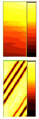
Speaking before the centennial meeting of the American Physical Society, Xiao-Dong Xiang, a physicist with Berkeley Lab's Materials Sciences Division, described how the SEMP uses near-field or non-propagating microwaves (as opposed to normal far-field microwaves such as radar) to measure the electrical impedance of materials with sub-micron resolution. For the electronics industry, a material's electrical impedance – a measurement of its ability to conduct an alternating current – is its most critical property. "The SEMP is capable of mapping the complex electrical impedance of any material," says Xiang. "We chose the lower range microwave frequencies (a few GigaHertz) because this is the most relevant and best-suited range for most electronic applications." By measuring the interaction between evanescent microwaves generated off an ultra sharp-tipped probe and the surface of a material, Xiang and his colleagues can not only map electrical impedance across the face of the material, they can at the same time map the topography of the material's surface, another critical factor for manufacturing chips and other electronic devices. The SEMP's sharp-tipped metal probe is connected to a high quality-factor (Q) microwave resonator equipped with a thin-metal shield. This shielding is specially designed to screen out all but the evanescent microwaves from being generated at the SEMP's tip. As a result, when the tip is scanned over a sample, just above the material's surface, only these evanescent microwaves, with their high spatial resolving power, are free to interact with the sample. "This feature is crucial for high resolution quantitative microscopy," says Xiang. "If both evanescent and propagating microwaves had to be considered and calculated, as is the case for all other types of microwave probes, the quantitative microscopy would be impossible." The interaction between the evanescent microwaves and the sample surface gives rise to a resonant frequency and quality-factor changes in the resonator that are recorded as signals. Xiang and his colleagues can measure these change signals and plug the measurements into equations they've developed which translates the results into a measurement of the sample's complex electrical impedance with a spatial resolution of 100 nanometers. The SEMP can be used on conductors and insulators as well as semiconductors. It has applications in any situation in which there is a need to characterize a material's electrical properties as a function of electric or magnetic fields, optical illumination, or temperature variations. The Berkeley Lab researchers have employed "tip-to-sample distance feedback control techniques" to obtain topographical and electrical measurements of sample surfaces – important for mapping electrical impedance without contacting the sample surface. "Since the feedback control ranges from nanometers to microns, the SEMP has a zoom-out feature that allows it to scan a large area in a short amount of time, and a zoom-in feature that allows it to scan a small area with high resolution," says Xiang. "These features make the SEMP a practical tool for industrial applications." Working with Xiang on the development of the SEMP were Tao Wei, Chen Gao, Fred Duewer, and Ichiro Takeuchi. Although the basic technology behind the SEMP has been licensed to Ariel Technologies, Inc., Xiang and his colleagues are continuing to refine and expand it. They are currently building a low-temperature version which will allow them to study superconductors. Berkeley Lab is a U.S. Department of Energy national laboratory located in Berkeley, California. It conducts unclassified scientific research and is managed by the University of California. |