|
|
 |
In what was hailed as the next major advance in the evolution
of integrated circuits, a consortium of industry and government
laboratories, including Berkeley Lab, has announced completion
of the first full-scale prototype machine which demonstrates
all critical capabilities for making computer chips using
extreme ultraviolet (EUV) light. This breakthrough will
lead to microprocessors that are 10 times faster than
today's most powerful chips and create memory chips with
similar increases in storage capacity.
Akin to photography, lithography is used to print circuits
onto microchips. EUV lithography is being developed because
the current chip-printing technology is expected to reach
its physical limits in the next few years. The consortium
includes Berkeley Lab, Sandi-California National Laboratory,
Lawrence Livermore National Laboratories, Intel, Motorola,
Advanced Micro Devices, Micron Technology, Infineon Technologies
and IBM.
Current lithography technology is expected to allow manufacturers
to eventually print circuits as small as 0.1 micron in
width, or 1/1,000th the width of a human hair. EUV lithography
technology is being developed to allow semiconductor manufacturers
to print circuit lines well below 0.1 micron -- down to
at least 0.03 microns (30 nanometers), extending the current
pace of semiconductor innovation at least through the
end of this decade.
Processors built using EUV technology are expected to reach speeds of
up to 10 gigahertz (GHz) in 2007. By comparison, the fastest Pentium 4
processor today is 1.5 GHz.
The successful prototype machine, called the Engineering
Test Stand, was built in Livermore. Here at Berkeley Lab,
the Lab's Center for X-ray Optics provided the essential
measurements that enabled the printing of the first tiny
lithographic circuits in January. The center is headed
by David Attwood.
Said Attwood, "We have a saying in optics: if you
can measure it, you can make it. New technology at new
wavelengths requires expertise in optics, and our specialty
(soft x-rays) perfectly fit the needs of the system."

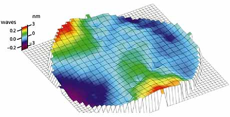
AT BERKELEY LAB, RESEARCHERS DETECT FLAWS IN THE OPTICS
AS SMALL AS THE RADIUS OF A HYDROGEN ATOM. IN
THE CASE OF THE ABOVE OPTIC, HEIGHT -- ABOUT 13.4 NANOMETERS
-- IS A MEASURE OF THE OPTIC'S DEVIATION FROM PERFECT
SHAPE.
The Center for X-ray Optics operates three beamlines
at the Lab's Advanced Light Source (ALS). As observed
by Gen. John Gordon, Administrator for the DOE's National
Nuclear Security Administration, "The ALS produces
light used to make measurements that are not possible
anywhere else."
To give an idea of size, scientists had to study features
that were in some cases 20 to 40 atoms across. The interferometry
developed at the ALS -- the most accurate wavefront measuring
device in the world, Attwood says -- allowed them to increase
the accuracy of the EUV wavelength to about 0.4 angstroms,
measuring deviations smaller than the radius of a hydrogen
atom. The multilayered molybdenum-silicon coating,
the enabling technology for the lithography process, comes
in at around 67 angstroms per layer -- half a wavelength.
Finding one defect on a printing mask, which the ALS can
also do, is equivalent to searching for a golf ball in
an area the size of Rhode Island.
 |

BEAMLINE 12.0 AT THE ADVANCED LIGHT SOURCE WHERE
THE EUV LITHOGRAPHY TEAM INCLUDES (FROM LEFT) KEN
GOLDBERG, JEFF BOKOR, AND PATRICK NAULLEAU.
|
The goal is to etch ever-smaller features on silicon wafers. It is done
in vacuum using laser-generated plasma to produce light that cannot be
seen with the human eye, and using highly sophisticated mirrors that serve
as lenses to project computer chip patterns onto silicon wafers. EUV
technology is "the leading horse in the race" for
next-generation lithography technology in the industry, according to Intel
CEO Craig Barrett.
The three laboratories and industry partners -- more than 200 people --
have been working closely on this technology since a Cooperative Research
and Development Agreement (CRADA) was signed in 1997. They intensively
followed up on relevant research whose earliest publication was 1989. The
labs formed a Virtual National Laboratory, which has since been a model
for similar collaborations. The industry group created a limited liability
company to manage the investments.
Berkeley Lab's metrology effort involved three teams.
The first, on beamline 6.3.2., focused on those critical
layered coatings and their reflectivity. This group was
led by Jim Underwood, one of the pioneers of the coating
process, plus Eric Gullikson and Stan Mrowka. "The
Berkeley and Livermore teams worked three shifts a day,
six days a week, night and day for four years," Attwood
said of the group's commitment.
 |

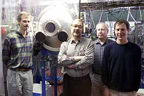
PICTURED HERE (LEFT TO RIGHT) ARE ERIC GULLIKSON,
JIM UNDERWOOD, STAN MROWKA AND BENJAMIN KAUFMAN
|
The interferometry team at beamline 12.0 included the late Hector
Medecki, Jeff Bokor, Ken Goldberg, Patrick Naulleau, and former student
Edita Tejnil, now with Intel. They are now working on the second
generation of optics from Tinsley Labs of Richmond as they study improved
optics for commercial applications. "The world's best optics meets
the world's best interferometer," Attwood says.
Beamline 11.3, dedicated to finding defects in the mask patterns, is
staffed by Moonsuk Yi of Korea, Tsuneyuki Haga from Japan, and Bokor, a UC
Berkeley professor.
As the CRADA with the computer companies completes its fifth year, the
three laboratories will improve and refine the test stand machine, a
10-by-10-foot box which sits in a clean room at Sandia. Eventually, the
pre-commercial work will be turned over to manufacturers, and if all goes
according to plan, by around 2007 we will see super-small, super-fast
computers with capabilities for universal language translation,
unprecedented medical and biological analysis, nascent artificial
intelligence, and voice commands.
Through it all, Attwood said, Berkeley Lab will remain
active as the reference standard for EUV metrologies.

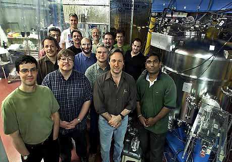
RESEARCH TEAM, PICTURED AT THE ADVANCED
LIGHT SOURCE
Additional information:
|


