| lab a-z index | phone book |
| May 20, 2005 | news releases | receive our news releases by email | science@berkeley lab |
|
|||
|
|||
| A Few Steps Closer to Nanoscale Photonic Technology | |||||||||||||||||||||||||
| Contact: Lynn Yarris (510) 486-5375, lcyarris@lbl.gov | |||||||||||||||||||||||||
|
BERKELEY, CA – One day our electronic technology, which is based on the manipulation of electrons, could be supplanted by photonics, which is based on the manipulation of light waves (photons). If the promise of photonic technology is realized, the high-speed processing and movement of data today will seem so sludgelike, people of the future will wonder how we ever got anything done. Photonic technology is still a long way down the road but the goal is a few steps closer now. Scientists with the U.S. Department of Energy’s Lawrence Berkeley National Laboratory (Berkeley Lab) and the University of California at Berkeley, working with free-standing, chemically synthesized nanowires and nanoribbons, have been able to guide pulses of laser light through a variety of complex structures. They have even, for the first time ever, been able to send those pulses within a liquid.
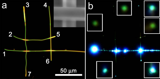
“We’ve been able to assemble nanowire lasers and semiconductor nanoribbon waveguides into multi-wire model structures that illustrate how light can be transmitted between active and passive nanoscale diameter cavities,” said Peidong Yang, a chemist with Berkeley Lab’s Materials Sciences Division, and a professor with UC Berkeley’s Chemistry Department, who led this research. “We’ve also introduced a major new application area for nanoribbons and nanowires as nanoscale optical waveguides in a liquid media, which holds importance for microfluidics and biology.” Yang and his research group are at the forefront in the development of semiconductor nanowires and nanoribbons, single crystals that can measure a millimeter in length, but only a few hundred or less nanometers in width and thickness (about one ten-millionth of an inch). They’ve demonstrated that these nano-sized ribbons can serve as “waveguides” for channeling and directing the movement of light waves through circuitry. Integrated circuitry on a nanoscale (a thousand times smaller than today’s microcircuits) is a critical requirement for photonic technology. “Over the past couple of years, we’ve worked heavily towards using nanowires as building blocks for the purpose of photonic applications,” Yang said. “So far, we’ve made nanoscale lasers, photodetectors, and ribbons that serve as flexible sub-wavelength optical waveguides. Ultimately, we want to integrate all these individual components together into a photonic system-on-a-chip that could be used to perform instant and detailed analyses for studies in chemistry, biology and medicine.” In the May 20, 2005 edition of the Proceedings of the National Academy of Sciences (PNAS), Yang and several collaborators report on the coupling of nanowire lasers, made from either gallium nitride or zinc oxide, to nanoribbons, made from tin oxide, a semiconductor of keen technological interest for its exceptional potential to be used to transport both photons and electrons in nanoscale components. The nanowire lasers, which were developed by Yang’s research group, are pure nanosized crystals that emit coherent ultraviolet light via a process called “optical pumping.” In the PNAS paper, Yang and his co-authors show that it is possible to transport individual pulses of laser light from the nanowires to the ribbon waveguides, a prerequisite if photonic devices are to be useful in communications or computing applications. They also demonstrate that networks of the tin oxide nanoribbons can be used as multi-channel filters for separating the component colors of white light and routing them through individual channels. In addition, they report on the creation of an optical crossbar grid made of two pairs of orthogonal ribbons that conducted light through abrupt 90 angles, analogous to the cross-bars in nanowire electronics. Such crossbars, the authors suggest, could form the basis of optical nanowire logic.
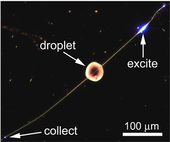
Perhaps the most intriguing of the results reported in the PNAS paper was the demonstration by the authors that their high refractive-index nanowires and nanoribbons can be used to guide light in water and other liquids. In one test, the tip of a nanoribbon was embedded with a droplet of laser dye, and a nanopulse of blue light was then sent into the far end of the ribbon. This produced a strong fluorescence from within the droplet, a fraction of which was captured by the ribbon cavity and guided back to the ribbon’s far end, proving that these waveguides are capable of routing signals both to and from liquids. “The fact that the wave guiding ability of our freestanding, flexible wires and ribbons survives in liquid media suggests a role for nanowire light delivery in integrated on-chip chemical analysis and biological spectroscopy,” said Yang. “Light guided by a nanoribbon could be used to sense fluorophores located at the end of the ribbon and in the evanescent field along its surface. Absorbance sensing might also be possible by launching broadband light through a nanoribbon in contact with picoliter volumes of solution.” The incredible potential of photonics can be glimpsed in today’s fiber-optic communications, where a single optical fiber can carry the equivalent of 300,000 telephone calls at the same time. But the power of fully realized photonics goes far beyond this. Whereas electrons must carry information sequentially, one electron at a time, with photons of light, there’s virtually no limit to the number of information packets that can simultaneously be transmitted. For example, it’s been estimated that a photonic Internet could transmit data at 160 gigabits per second, which is thousands of times faster than today’s typical high-speed connection. Another possibility is the optical computer, which could solve problems in seconds that would take today’s electronic computers months or even years to solve.
The timeframe for when nanoscale photonic technology will be ready for primetime consumption is difficult to predict, as a number of issues must first be resolved, including the need for a way to chemically synthesize geometrically precise nanowires and nanoribbons in mass quantities. Yang and his group are exploring several promising techniques for accomplishing this, including the use of optical traps, and a hybrid bottom-up/top-down approach. “I think we could soon be seeing commercial application of nanowires and nanoribbons in areas that require less integration, such as sensing and energy conversion,” Yang said. “However, for applications that require a high level of integration, it will take much longer.” Co-authoring the PNAS paper with Yang were Donald Sirbuly, Matt Law, Peter Pauzauskie, Haoquan Yan, Alex Maslov, Kelly Knutsen, Cun-Zheng Ning and Richard Saykally. Maslov and Ning are with the NASA Ames Research Center, the others are with Berkeley Lab and/or UC Berkeley. This work was supported in part by the Camille and Henry Dreyfus Foundation, the Beckman Foundation, and the U.S. Department of Energy. Berkeley Lab is a U.S. Department of Energy national laboratory located in Berkeley, California. It conducts unclassified scientific research and is managed by the University of California. Visit our Website at www.lbl.gov. |
|||||||||||||||||||||||||
| Top | |||||||||||||||||||||||||