| lab a-z index | phone book |
| February 27, 2006 | news releases | receive our news releases by email | science@berkeley lab |
|
|||
|
|||
Nanoscale Tubing Assembles Itself Instantly |
||||||||||||||||
| Contact: Paul Preuss, (510) 486-6249, paul_preuss@lbl.gov | ||||||||||||||||
BERKELEY, CA —Making tubes useful often means joining them to other tubes and linking them together in networks. Easy enough to do with standard water pipes — but on the nanoscale, joining nanotubes is hard to do. Efforts to link nanotubes have usually begun with the most familiar kind, cylinders whose structure is equivalent to one or more rolled-up sheets of a layered crystal like graphite. Now researchers at Lawrence Berkeley National Laboratory's National Center for Electron Microscopy (NCEM) and the Christian Albrechts University of Kiel, Germany, have found a completely new way to form complex networks of nanotubes. The researchers describe their results in the March 3, 2006 issue of Physical Review Letters, now available online.
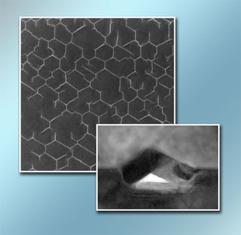
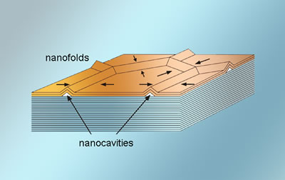
The new method causes extensive hexagonal networks of tubes, intricately branched and connected, to form in less than a second on the surface of a layered crystal. The tubes themselves are prismatic folds, having the cross section of a pitched roof. Erdmann Spiecker of Berkeley Lab's Materials Sciences Division, on leave from the University of Kiel, led the team that analyzed the nanofold network phenomenon. Spiecker is a member of the group headed by Wolfgang Jäger in Kiel, where colleagues from another group first observed the mysterious networks when they deposited metal atoms on the surfaces of layered crystals of titanium telluride and vanadium selenide (materials known as transition metal dichalcogenides). "Originally it was thought the structures were cracks, like cracks in the mud of a dry lake bed, which filled up with the condensed metal to form nanowires," Spiecker says. "We started to question this idea when we failed to find evidence of condensed metal anywhere in the samples." Other models were considered, including the networks of wrinkles that can form in layers of plastic or foil on a window pane, but there were problems with these mechanisms as well. Spiecker got support from the U.S. Department of Energy and the German Science Foundation to investigate the phenomenon at Berkeley Lab's NCEM. NCEM's director Ulrich Dahmen says, "We have many unique resources here — including a focused ion beam facility, a custom-built low-energy electron microscope, and several high-resolution microscopes — but they often tend to follow their own program tracks. To Erdmann these boundaries didn't exist. He brought the equipment and the skills together to solve an unusual scientific problem." Barely Skin DeepTransmission electron microscopy (TEM) of the vanadium selenide crystals, which looks all the way through the sample, revealed moiré patterns, a clue that the real nature of the networks involved altered spacings between atoms in the crystalline layers near the surface of the material. Like layers of graphite, in which carbon atoms are tightly bonded in two dimensions but weakly bonded between layers, vanadium selenide also consists of layers of atoms tightly bonded in the plane and weakly bonded between layers. But vanadium selenide's two kinds of atoms can combine in different lattice geometries within each layer. To discover what was going on in these layers during surface network formation, Spiecker and his colleagues turned to NCEM's low-energy electron microscope (LEEM). "The LEEM is made to study surfaces, using a beam with an energy of a few electron volts, which penetrates only a few layers," explains NCEM's Andreas Schmid. "Our LEEM has an ultra-high-vacuum sample chamber, orders of magnitude better than most other electron microscopes, so contaminating molecules don't affect the sample's surface." In the LEEM's high-vacuum chamber the researchers cleaved a vanadium selenide crystal to expose a smooth, fresh surface. Then an area some seven millionths of a meter across, about the diameter of a red blood cell, was videotaped at the rate of one frame per second while copper atoms were slowly deposited from vapor. For 13 minutes nothing happened. Then, between one video frame and the next, the network abruptly formed. Next the researchers sliced the sample crossways with a focused ion beam (FIB) to find out what the network elements looked like from the side. NCEM's Andrew Minor devised a "shadow FIB" technique that eliminated the chance of distortion. He explains, "Instead of applying a protective layer of platinum, which would have ruined what we wanted to look at, we preserved the surface layers intact by using the ion beam to shave away unwanted material from the back of the sample." With high-resolution transmission electron microscopy, the researchers then showed that the network was formed of hollow nanofolds in the surface layers, which had been pushed together to form roof-like structures. Plan views of the sample with high-resolution TEM mapped the nanofold network as well as identifying the positions of copper atoms in the layers beneath the surface. Rather than building up on the surface, the copper atoms had worked their way into the uppermost layers and lodged between them, forming what’s called an "intercalation compound."
"We believe we are observing a chemical reaction, involving a phase change in the lattice structure of the surface layers," Spiecker says. "Kinetic energy is much too small for the metal atoms to penetrate into the crystal." As the copper atoms accumulate and change the structure of the layers they create compressive stress, literally pushing the surface layers sideways in every direction until they abruptly break free, gliding over the underlying layers and crinkling themselves into a hexagonal network. Questions and PossibilitiesWhile much of the mystery has been solved, Spiecker points out that numerous intriguing scientific questions remain, beginning with how fast the networks form. "By adjusting the video frame rate we may be able to detect the interval between no network and a fully formed network with one-tenth of a second time-resolution, but we can't resolve the dynamics on the microsecond scale," says Spiecker. "We'll have to come up with new methods to do that." Other fundamental questions include what conditions trigger the sudden release of strain, and how the several layers of crystal that make up the nanotube roofs compensate for the different stresses experienced by the inner and outer layers where they bend. There are many practical questions as well. Surface nanotube networks suggest numerous applications, including networks of pipes for the storage and transport of minute quantities of materials, or templates for the fabrication of nanowire networks. "There are many exciting follow-ups to investigate in these systems," says Dahmen, "ranging from whether and how the tubes can be filled with liquids or with metal atoms to form wires, to controlling the sizes and patterns of the networks, to understanding the atomic structure of their junctions." The whole process, Minor remarks, "is an example of how NCEM is supposed to work — bringing together instruments and expertise from many different specialities to address a fascinating set of problems." "Self-Assembled Nanofold Network Formation on Layered Crystal Surfaces During Metal Intercalation," by E. Spiecker, A. K. Schmid, A. M. Minor, U. Dahmen, S. Hollensteiner, and W. Jäger, appears in the March 3, 2006 issue of Physical Review Letters and is available online to subscribers. Berkeley Lab is a U.S. Department of Energy national laboratory located in Berkeley, California. It conducts unclassified scientific research and is managed by the University of California. Visit our website at http://www.lbl.gov. |
||||||||||||||||
| Top | ||||||||||||||||