| lab a-z index | phone book |
| March 29, 2006 | news releases | receive our news releases by email | science@berkeley lab |
|
|||
|
|||
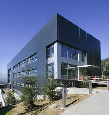
Berkeley Lab Dedicates the Molecular Foundry |
||||||||||||||||
| Contact: Lynn Yarris (510) 486-5375, lcyarris@lbl.gov | ||||||||||||||||
BERKELEY, CA — Traditionally, a foundry has been a place where molded objects are made. The term comes from “founding,” the act of pouring a liquid material into a mold and allowing it to solidify. Since the introduction of industrial foundries in the 17th century, the shape and size of the objects that can be made at a foundry has been limited only by the ability to liquefy a material and cast it in a mold. At a foundry where objects can be fashioned atom-by-atom or molecule-by-molecule, the potential shapes and sizes are virtually limitless. This is the promise of the Molecular Foundry that was officially dedicated at the Lawrence Berkeley National Laboratory (Berkeley Lab) on March 24, 2006.
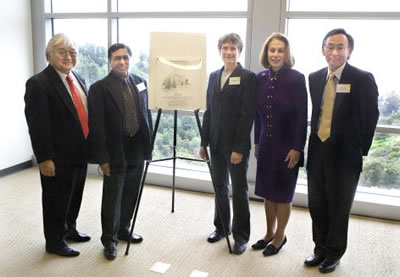
“The Molecular Foundry has nanoscale research capabilities not found at any other facility,” said Foundry director Carolyn Bertozzi at the dedication ceremony. “It creates an environment in which scientists from different disciplines can work together under one roof to expand our knowledge of the nature of matter on a nanoscale.” “The dedication of the Molecular Foundry represents a milestone in the field of nanoscience,” said Paul Alivisatos, Berkeley Lab’s Associate Director for Physical Science and an international authority on inorganic nanocrystals, who will head the Foundry’s inorganic nanostructures research program. The Molecular Foundry is the first of five proposed U.S. Department of Energy Nanoscale Science Research Centers and the only one on the West Coast. It is housed inside an $85 million, six-story, 94,500 square-foot steel and glass building. The building was designed by the SmithGroup of San Francisco, and constructed by Rudolph and Sletten General Contractors, out of Foster City, working in close collaboration with Berkeley Lab staff, including Jim Krupnick, the construction project director, and Joe Harkins, the construction project manager. Ground for this facility was broken only two years ago. As a DOE national research facility, the resources at the Molecular Foundry will be made available to qualified scientists throughout the country. Already, more than 50 Molecular Foundry scientific projects have been approved. The dedication ceremony was held in the Foundry’s fifth floor Cantilever Room, which offers a spectacular view of the San Francisco Bay. On hand to help celebrate the occasion, in addition to Bertozzi and Alivisatos, were Berkeley Lab director Steven Chu, Sunne McPeak, Secretary for Business, Transportation and Housing for the State of California, Altaf Carim, from DOE’s Office of Science, and Congressman Mike Honda, who represents Silicon Valley and was a co-sponsor of the 21st Century Nanotechnology Research and Development Act. Said Lab Director Chu in his welcoming remarks, “The Molecular Foundry represents a concerted effort to bring together all that we have learned about nanoscale materials and properties. This dedication today is a wonderful way to celebrate an idea that began more than a decade ago with our own Daniel Chemla.” Chemla, a leading authority on the optical and electronic properties of nanoscale materials, now retired, proposed the Molecular Foundry as a way to “change the paradigm for nanoscale materials research.” He attended the dedication ceremony along with his wife, Berit. Technology at the nanometer scale is not simply today’s microtechnology only smaller. At the nanoscale, which is one thousand times smaller than the microscale, matter exhibits very special properties because of quantum size effects, altered thermodynamics, and modified chemical reactivity. This presents special scientific challenges that the facilities at the Molecular Foundry are uniquely designed to meet. It is expected that the state-of-the art design and energy efficiency technologies used in the construction of the Molecular Foundry will result in its becoming the first Berkeley Lab building to receive a prestigious LEED Silver rating from the U.S. Green Building Council. Qualifying a scientific research laboratory building for a LEED Silver rating is difficult because of the high energy use such facilities typically incur. However, the Molecular Foundry is projected to consume 30-percent less energy than the already-stringent California requirement for laboratory buildings.
Research at the Molecular Foundry will encompass “hard” (inorganic) materials, including nanocrystals, nanotubes, and lithographically patterned structures, and “soft” (organic and biologic) materials, such as polymers, DNA, proteins, and components of living cells. Nanometer lengths-of-scale are where investigations into hard and soft materials meet and to study this common ground, researchers at The Molecular Foundry will invoke the primary fabrication strategies of both — the “top-down” approach practiced by solid-state physicists and physical chemists in which existing structures and objects, such as semiconductors, are made smaller; and the “bottom-up” approach practiced by chemists and molecular biologists in which atoms and molecules are connected together to make larger structures and objects. The Molecular Foundry will host its own research program and collaborative programs with visiting researchers, and will also provide training for graduate and post-doctoral students. In addition to its research programs and training component, The Molecular Foundry will also serve its collaborators as a “portal” into three other national user facilities at Berkeley Lab, each of which offers cutting-edge technical capabilities crucial to effective nano-scale research. These three facilities are: the Advanced Light Source, a synchrotron storage ring that generates some of the brightest and most intense x-rays available for scientific research; the National Center for Electron Microscopy (NCEM), where researchers can “see” atoms in a crystal and have achieved sub-angstrom resolutions of structural details; and the National Energy Research Scientific Computing Center (NERSC), which is one of the most powerful computing resources for non-classified research in the world. Among the possible developments foreseen for the Molecular Foundry are the fabrication of electronic devices out of carbon nanotubes; the detection and treatment of diseases at the cellular level; the reduction of waste and pollution in manufacturing processes; improved sensors for real-time monitoring of chemical and biological activity; high-performance electricity transmission lines and next-generation solar cells. Berkeley Lab is a U.S. Department of Energy national laboratory located in Berkeley, California. It conducts unclassified scientific research and is managed by the University of California. Visit our Website at www.lbl.gov. Additional Information
|
||||||||||||||||
| Top | ||||||||||||||||