|
June 4, 2002
|
|
 |
 |
| What the numbers mean | ||
| Contact: Paul Preuss, paul_preuss@lbl.gov | ||
|
|
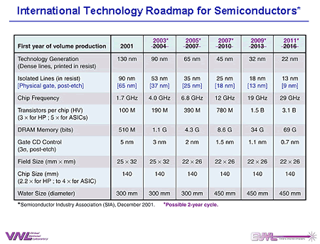
The Semiconductor Industry Association periodically outlines future prospects and challenges in a technology "roadmap." Anticipated milestones are called "nodes," defined as a bi-yearly reduction in the size of commercially manufactured chips leading to an increase in chip density by a factor of two.
Nodes are expressed as distances in nanometers, billionths of a meter -- half the distance, or pitch, between lines in a set of equally wide, equally spaced lines etched into a chip like a DRAM (dynamic random access memory) or MPU (microprocessor unit). Nodes at 90 nm, 65 nm, 45 nm, and 32 nm are expected to be reached within the decade. But David Attwood, former head of the Center for X-Ray Optics and leader of Berkeley Lab's extreme ultraviolet lithography program, says that "actual transistor gate widths are considerably narrower than the node number, which are half periods of equal lines and spaces printed with a given optical system, or 'stepper.'"
Attwood explains that "by using materials processing tricks such as exposure thresholds and development nonlinearities, narrower lines are printed as electronic gates. Thus in fact, lines narrower than the wavelength of the light used to print the chips are achieved. For example, in late 2001, 80 to 90 nm wide gate widths were being printed with 248 nm light, certainly less than the wavelength. This may have also included some use of clever optical wavefront engineering -- 'phase tricks' -- but I believe the major 'trick' is materials processing. Quite amazing when you consider that they do this in high volume manufacturing." Attwood cites examples in the 2001 edition of the International Technology Roadmap for Semiconductors: "The 2001 node is 130 nm, but the isolated line in resist [an intermediate stage of chip processing] is narrowed to 90 nm, and the metalized gate after processing is down to 65 nm. This is the physical gate width in the transistors that permits the achievement of 1.7 gigahertz clock speed." Clock speed, measured in cycles per second (a gigahertz, abbreviated GHz, is a billion cycles per second), is the rate at which a computer processor executes instructions and is often used as a rough estimate of computer power. By spring 2002, top-of-the-line commercial processors had reached a clock speed of 2.4 GHz. "Projected forward to the 32 nm node, which is likely to arrive in 2009, the isolated lines in resist are projected to be 18 nm, narrowed to 13 nm in the final metalization process, which would give a projected clock speed of 19 GHz," says Attwood. Referring to test wafers printed by the SES at the Advanced Light Source, Attwood says, "So where do the EUV 39 nm line widths printed at the ALS fit in? These are isolated lines printed in resist by Patrick Naulleau and his team, using an EUV optical system of 0.1 NA at 13.4 nm wavelength." NA means numerical aperture; somewhat like f-stop in ordinary cameras, NA measures the amount of light that can pass through the system. Future EUV optical systems, one hopefully at the ALS next year, will be at 0.25 to 0.3 NA, providing better resolution and taking us to about 16 nm line widths in resist -- a perfect match to the 32 nm node in 2009." Attwood concludes, "Clearly we have a great future here and are
making a major contribution to the technological leadership and economic
health of the U.S." Additional information:
|
||||||||||||||||