
Molecular
Foundy Begins Reign with Shovel of Dirt
President's 2005 Budget:
Science Funding Flat, Lab Priorities Supported
Molecular Foundry Begins Reign with Shovel of Dirt
BY LYNN YARRIS
 |
|
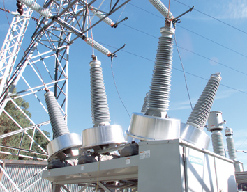
| Rainy weather forced (left to right) Rep. Mike Honda, Paul Alivisatos, Pat Dehmer of the DOE, Sean Randoph of the Bay Area Economic Forum, and Director Charles Shank indoors to symbolically break ground for the Molecular Foundry. | |
“It’s a Small Small World” might have been an appropriate theme-song at Berkeley Lab last week, but the focus of attention was anything but kids’ stuff. Friday, Jan. 30, saw ground officially broken for construction of the Molecular Foundry, an $85 million, six-story, 94,500 square-foot building that will serve as a DOE national user facility aimed at the development of nanotechnology. The preceding day saw the convening of the first Molecular Foundry user workshop.
“Berkeley Lab has been a pioneer in developing materials on the nano-scale, and our Molecular Foundry is going to help open new doors to humankind,” said Berkeley Lab Director Charles Shank in his welcoming remarks at the groundbreaking ceremony. “We’re setting off on an adventure that I believe has virtually limitless possibilities.”
Because of early morning rain, the groundbreaking ceremony took place inside the Building 66 auditorium, using a trough of dirt from the actual construction site which could be seen out the auditorium window. The auditorium was filled to capacity and the audience included representatives from the U.S. Department of Energy (DOE), the University of California, and top Bay Area R&D institutes. There were also members of the media, including the Oakland Tribune, San Francisco Chronicle, San Jose Mercury News, and KGO-TV.
The featured speaker was U.S. Representative Mike Honda (D-San Jose), cosponsor of the Nanotechnology Act of 2003, which authorized $3.7 billion over the next three years for nanotechnology research and development programs. Eying the trough of dirt as he stepped up to the podium, Honda joked, “I thought there must be a cat in here.”
Turning serious, Congressman Honda spoke as a policy maker to the importance of educating the public about nanotechnology. “It takes an entire community to move a technology forward and we need to ensure that no one gets left behind,” he said. “There will always be nay-sayers who would like to stop all technological progress so we must work hard to inform other members of society and bring them along.”
Honda invited scientists to “team up with policy makers such as myself so together we can make Bay Area nanoresearch the crucible for the future.”
He then added, “I wish I were 18 all over again so that I could see more of this exciting future.”
 |
|
| Nanosys chair Larry Bock. |
Also speaking at the ceremonies were Pat Dehmer, Associate Director of DOE’s Basic Energy Sciences program; Sean Randolph, president of the Bay Area Economic Forum; and Molecular Foundry Director Paul Alivisatos. Dehmer described the “extreme enthusiasm” of Energy Secretary Spencer Abraham for nano-science, and said he wants a national “nanosummit” in the near future. She also joined Alivisatos in acknowledging that the Molecular Foundry began as the vision of Daniel Chemla, director of Berkeley Lab’s Advanced Light Source.
Randolph took the opportunity to introduce a 36-page report prepared under the auspices of BASIC (Bay Area Science and Innovation Consortium) entitled “Nanotechnology in the San Francisco Bay Area: Dawn of a New Age.” The report is an introduction to nanoscience in the Bay Area for the general public.
“Since the collapse of the dotcom bubble, much has been written about the death of the Bay Area economy,” said Randolph. “But the Bay Area continues to create new paradigms in which our economy moves forward to the next step. Today, nanotechnology may be that next step.”
Prior to the groundbreaking ceremony, a keynote address was given for the users workshop by Larry Bock, executive chairman of the board of Nanosys, Inc. His talk, entitled “Why Nano? Why Now?,” delighted his audience. At one point, Bock showed a clip from a scene in the 1967 movie, The Graduate, in which a young Dustin Hoffman is given career advice in a single word. Only instead of the famous “Plastics!” in Bock’s clip the word was “Nanotechnology!”
The central message of Bock’s talk was that nanotechnology is not just smaller, it’s different. Arguing it is more closely related to biotechnology than microtechnology, Bock said we can expect to see entirely new technological phenomena emerge from nanoscience.
Noting that to date there’s been no “gold rush” of venture capitalists to fund nanoresearch, Bock gave a list of reasons, including economics, government regulations and the tradition of investors putting their money into ventures that have been done successfully before “with someone else’s money.”
However, he said, until now there’s never been a facility for
nanoresearch like the Molecular Foundry. Showing an artist’s
concept of how the Foundry will look upon completion, Bock concluded,
“Nano starts here.”
Photo: groundbreaking-shovels.jpg
Rainy weather forced (left to right) Rep. Mike Honda, Paul Alivisatos,
Pat Dehmer of the DOE, Sean Randoph of the Bay Area Economic Forum,
and Director Charles Shank indoors to symbolically break ground for
the Molecular Foundry.
President's 2005 Budget: Science Funding Flat, Lab Priorities Supported
 |
|
| Spencer Abraham | |
Speaking with the press, the Secre-tary reiterated the Administration’s support of DOE’s science programs and facilities. When accounting for the expiration of many congressionally earmarked projects, the Office of Science’s budget request is basically flat at approximately $3.4 billion. Berkeley Lab’s budget is also expected to remain flat, but contains funding for many of the Lab’s priorities, including:
- Funding for construction of the Molecular Foundry is to continue at $32 million and completion is still targeted for FY 2006.
- Increasing computing and user capabilities at NERSC is promoted with a $6 million increase in funding.
- SNAP is noted as the Depart-ment’s most promising science program to answer the question, “What is dark energy?” Funding for this program is approximately $7.6 million potentially, with additional funding from NASA.
- Infrastructure improvements at Berkeley Lab will also continue with $4.8 million for rehabilitation of Building 77 and an additional $1.36 million for continued deconstruction of the Bevatron’s External Proton Beamline complex.
- The Lab’s Center for Beam Physics is set to receive $3.9 million, $300,000 over FY 2004.
- The budget recognizes the important role of ESNet and retains funding at approximately $18.3 million.
- Berkeley Lab’s education and worker development programs should see a boost with an increase in overall DOE funding from $1.9 to $3.1 million for graduate/faculty fellowships.
With the mounting federal deficit keeping spending in check, DOE and Berkeley Lab faired better than many domestic programs. Some agencies, such as the EPA, are proposing significant cuts up to 7 percent of their budgets.
A Step Closer to the Optimum Solar Cell
BY PAUL PREUSS
 |
|
| Kin Man Yu, left, and Wladek Walukiewicz in the lab where they measure optical and photovoltaic effects. | |
In 2002 Kin Man Yu and Wladek Walukiewicz of the Materials Sciences Division,work-ing with colleagues from Berkeley Lab and other institutions, realized that it might be possible to create a solar cell that responds to the sun's full spectrum by stacking junctions of an alloy, indium gallium nitride, that could each respond to a different wavelength of light.
Now the researchers have found a new alloy that can respond to virtually the entire solar spectrum with a single junction.
“This isn't a multijunction material,” Walukiewicz says, “it's even more interesting: a multigap material” — a single semiconductor with multiple band gaps.
“The only thing the two materials have in common,” says Yu, “is that they both try to capture as much of the solar spectrum as possible.”
How solar cells work
Sunlight comes in many colors, from low-energy infrared photons to high-energy ultraviolet photons. Semiconductors respond only to narrow ranges of energies, corresponding to their characteristic band gaps.
The band gap is the energy, expressed in electron volts (eV), required to kick an electron from the valence band into the conduction band, where electrons are free to move. Forming an electric current requires a junction between n-type (negative) and p-type (positive) versions of the material. When photons are absorbed, electrons migrate toward the n-type side of the junction (and “holes” toward the p-type side).
The leading solar cell material, crystalline silicon, has a band gap of only about 1.1 eV; most solar photons are much more energetic, and although they are absorbed, most of their energy is wasted as heat. These cells are at best 25 percent efficient.
Discovering the multigap phenomenon
Stacking materials to capture photons with a wider range of energies is a difficult strategy, because of the need to match crystal lattices of materials with suitable energy gaps. The single-junction cell is the structural ideal.
“In 1960, Martin Wolf suggested that by introducing impurities with the right electronic properties into a semiconductor you could make a single–junction solar cell that absorbs more photons with different energies,” says Walukiewicz. “Sounds easy, but nobody knew how to do it.”
Then in 1999, Walukiewicz and others were working with researchers at DOE's National Renewable Energy Laboratory, who were building a three-junction cell.
“They needed a new material with a 1-eV band gap and a crystallattice structure that matched the other layers of the cell,” Walukiewicz explains. “They used gallium indium arsenide nitride alloys in which just a little nitrogen could achieve the desired band gap and an almost perfect lattice match.”
Walukiewicz showed that incorporating the small amount of nitrogen splits the conduction band into two parts; the gap to the lower band was 1 eV. Although othercharacteristics made this a poor solar cell material, the phenomenon was not forgotten.
A perfect mismatch
Introducing impurity atoms like nitrogen or oxygen, with a strongtendency to attract electrons, intosome semiconductors produces a “highly mismatched alloy” whoseelectronic peculiarities are causedby split band gaps.
In most cases the split occurs inside the conduction band — not much use for photovoltaics. But Walukiewicz and his colleagues predicted that adding oxygen impurities to zinc manganese tellurium (ZnMnTe) would produce well defined, widely split band gaps.
“Figuring out how to do this was not easy,” Yu says. “First we used ion beams to implant the oxygen, then we used pulsed laser melting to liquefy the ZnMnTe and recrystallize it rapidly.” The researchers were able to create single crystals whose top layer — only 0.2 microm- eters thick (a micrometer is a millionth of a meter) — held enough oxygen impurity atoms to split thematerial's normal band gap.
A deck of energy levels
Two separate conduction bands allow photons of three different energies to be absorbed. The difference between the new alloy's valence band and the lower of the split bands forms one gap (1.8 eV). The difference between the two split bands forms a second gap (0.7 eV). Finally, the difference between the valence band and the upper conducting band forms a third gap (2.6 eV).
Together, these respond to virtually the entire solar spectrum. The calculated ideal efficiency of a single-junction solar cell made with this material would be a remarkable 57 percent.
Yu admits that forming highly mismatched alloys is “challenging from a crystal-growth point of view,” but there is hope that crystals can be grown with a different method.
Meanwhile, says Walukiewicz, “we have tested a single junction of the material which has given us a photovoltaic response” — demonstrating the kind of three-bandsemiconductor needed for high-efficiency, single-junction solar cells.
“Diluted II-VI oxide semiconductors with multiple band gaps,” by Kin Man Yu, Wladek Walukiewicz, J. Wu, Wei Shan, and Jeff Beeman of Berkeley Lab, Mike Scarpulla and Oscar Dubon of Berkeley Lab and UC Berkeley, and Piotr Becla of MIT, appeared in Physical Review Letters, Dec. 12, 2003.
So What’s Up with all the 12-kV Switching Announcements?
BY MONICA FRIEDLANDER
 |
|
| Grizzly Peak Sub Station |
Once a seldom occurrence, the booming voice startling us with ominous-sounding warnings of “12 kV switching” is becoming increasingly familiar — and not so ominous anymore. Should we duck? Ignore? Not to worry, the lab electricians reassure us. No sparks are flying and no one will get zapped. In fact, a lot of the time the work is being done miles away by PG&E, usually on the other side of the Caldecott Tunnel.
Two banks of transformers on the Hill receive power from PG&E’s 115-kV transmission lines, step it down to 12 kV, and distribute it through multiple 12-kV feeders to a number of switching stations.
To play it safe, every time work is done either by PG&E or on the Hill that could possibly result in a power interruption, preventive measures are taken and Lab employees are alerted.
“When PG&E is switching, we’re turning off equipment, as requested by PG&E, to make sure the switching doesn’t trip the Laboratory,” explains Tim Murphy, the Lab’s maintenance supervisor.
This week, however, the work did take place on the Hill as the Lab was testing a 2-MW generator now being commissioned. During this type of work, electricians switch breakers as they transfer load from one bus to another. The Diesel generator, expected to be operational by February, is intended as a backup in the event of future power outages.
Most of these switchings, referred to as “hot transfers,” occur during upgrades or scheduled maintenance, and involve no power interruptions, says Mahesh Gupta, chief electrical engineer for the Lab. When the work is done here, Lab electricians isolate a piece of equipment, repair it, and put it back in the system. But there’s always a very small possibility of power loss, Gupta warns — hence the announcements.
“With PG&E there are so many unknowns, anything can go wrong. PG&E voltage can dip, and that’s outside of our control. Even though we do not expect any incidents, anything can happen and power loss can occur.”
With that in mind, Gupta and Murphy advise employee to take basic precautions. Saving the data on your computer is the most obvious such measure. Researchers need not quit their equipment, but they may want to be on standby and, in certain instances, make sure portable generators are available or cooling systems are in place and operational, as needed. Microscopes are very sensitive to voltage loss, Gupta also warns.
Because ALS work could be seriously affected should something go wrong during a transfer load, hot transfer switching is not done when the ALS is operational (same for the 88-Inch Cyclotron). Instead, Gupta says, electricians now wait for a scheduled shutdown of the ALS and the 88-Inch to do their work.
The 12kV switching announcements have boomed through Lab loudspeakers for some 15 years. Until last year, however, they were heard mostly when power to particular buildings was shut off. A serious incident last year, however, changed that. During the work that brought the Grizzly Substation online in February 2003, a faulty wire connection tripped off 20 percent of the Lab’s electricity for five minutes, causing serious problems for researchers.
“Since then we’re more adamant,” Murphy says. “We give 15 minutes’ notice each time anything is done that could affect power.” The announ-cements are made either by the fire dispatchers in Building 48 or by Murphy himself. Notices are also placed in “Today at Berkeley Lab.”
Should you still be concerned that a switch could affect your work, Murphy suggests you call the Work Request Center at X6274 during work hours, or else the 24- hour Facilities hotline at X5481.
Short Take
Former Lab Employee Featured in New Book on ‘Women in Space’
 |
|
| Julie Rodriguez Jones’ “Eclipse,” a digital airbrush “painting” from 2001. | |
Astronomically-inspired landscapes have always captured the imagination of Julie Rodriguez Jones, an artist and longtime Lab employee who was recently selected as one of 100 women to be featured in a newly released book entitled “Women Of Space: Cool Careers On The Final Frontier.”
“Science in general and astronomy in particular are metaphors for the vision and exploration into the unknown,” said Jones a few years ago, when her art was among the winning entries exhibited in a prestigious New York gallery show. Her work has continued to capture the imagination of scientists and artists alike ever since.
Jones left a 30-year career at the Lab in 2003 to resume her art career. She began her employment at the Lab in 1971 as a research technician in the Physics Division and later moved to Operations in 1978. Her interest in astronomy, however, goes back to when she was a young girl, Jones recalls.
Although inspired by real space images, such as those sent back by the Hubble Telescope, her work integrates web and software media to produce her own unique style of imagery. She explains that she “paints” using a mouse-controlled airbrush in Adobe Photoshop. Her art emphasizes space images such as supernova, nebula, and planets, and has received a variety of awards and honors.
Inclusion in “Women of Space” is especially meaningful to Jones. “I hope that this book will inspire young women to pursue a variety of space related careers,” she said. “From my own second career I hope to remind women that it is never too late to pursue one’s passion.”
Jones’ artwork can be viewed online at www.artsoul.homestead.com/AstronomicalArt.html.
To Help New York Times with Efficient New Building
BY ALLAN CHEN
 |
|
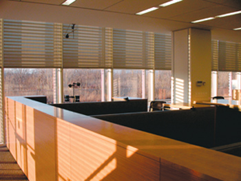
| Lab researchers are conducting tests at the Times' printing plant in College Point, NY, to prepare for construction of the paper's headquarters in Manhattan. |
The New York Times is building a new 52-story headquarters in the heart of Manhattan. In early 2003, representatives from the paper, along with members from its design and engineering contractors, visited the Lab’s Environmental Energy Technologies Division (EETD).
They spent a day learning about EETD’s research in energy efficiency, lighting and daylighting, glazing, and thermal comfort for commercial buildings from Stephen Selkowitz, Mary Ann Piette, Francis Rubinstein, Eleanor Lee, and others.
As a result of that visit, the New York Times Company and EETD have joined forces in a cooperative research project to test new technologies to increase the energy efficiency of the building, and to improve the indoor environment for the comfort of its occupants. The Times found it difficult to specify with confidence a costeffective, fully integrated glazing (window) and lighting control system, something EETD’s Building Tech-nologies staff has been researching for years.
New York Times Vice President David Thurm noted, “We were excited to find that Berkeley Lab’s prior work was relevant to our project. As an owner/operator, our primary interest is ensuring that the working environment in our building meets the comfort needs of our employees.”
 |
|
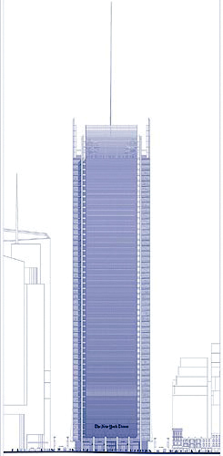
| Artist rendering of the New York Times’ new headquarters in Manhattan. | |
According to Selkowitz, this project is an opportunity to extend Berkeley Lab’s prior research to make more efficient and cost-effective systems available not only to the Times Company, but other owners and design teams as well, and to advance energy-efficient daylighting research.
“We’ve known since the 1970s that daylighting can reduce lighting energy use,” says Selkowitz. “But the mere use of large glass areas is not in itself a guarantee that energy savings or comfort will be achieved. It’s been difficult to make as much progress in the use of daylighting as we have in other areas. For one, daylighting requires a high level of system integration — designers have to design the building from the start to incorporate daylight into office spaces, there has to be a flexible and responsive control strategy to lower or turn off electric lights when daylight is available, and visual and thermal comfort must be maintained.”
Berkeley Lab research suggests that proper daylighting can reduce perimeter-zone lighting energy by as much as 60 to 70 percent of the annual electric-lighting energy with additional reductions in electricity demand. Overall building energy use can be reduced by 10 to 30 percent compared to a similar nondaylit building.
“In partnership with our team, led by Eleanor Lee, the Times has just completed a 4,500 square-foot test facility on the south and west quadrant of one floor of the building on the grounds of their printing plant in College Point, New York,” says Selkowitz. “This full-size mockup will allow us to demonstrate and test the key hardware, calibration and operational controls issues, allowing the team to specify a technological solution that meets comfort and energy-saving goals.”
Testing began at the mockup facility on Dec. 21, the winter solstice. While most of Berkeley Lab celebrated the holidays at home, Lee and her team were anxiously monitoring the data flow from the mockup.
The project is being funded by the New York Times Company and the
New York State Energy Research and Development Administration (NYSERDA),
with cost share from DOE and the CEC.
Protein Crystallographers Get Help From ELVES
BY LYNN YARRIS
 |
|
| ALS protein crystallographer James Holton says his software’s becoming so popular, his name tag at conferences should read “ELVES guy.” |
As everyone who has seen the Lord of the Rings films or read J.R.R. Tolkein’s works knows, when something had to be done quickly and efficiently, Middle Earthers turned to the elves. Now, modern protein crystallographers may soon be doing the same. ELVES is the name of an “expert system” of computer software programs that can automatically generate 3-D high resolution images of proteins from x-ray diffraction data. The system was developed by a Berkeley Lab scientist working at one of the protein crystallography beamlines of the Advan-ced Light Source (ALS).
“ELVES decreases the time and training required to perform the computational steps of x-ray crystallography and increases the efficiency of protein crystallography beamlines at synchrotron sources like the ALS,” explains James Holton of Berkeley Lab’s Physical Bioscien-ces Division, who mainly developed ELVES while still a graduate student at UC Berkeley. “This in turn should facilitate projects in structural geno-mics and biology.”
Holton is in charge of operations at ALS Beamline 8.3.1, an experimental facility powered by hard xrays (2.4 to 15 keV) off a Superbend magnet that’s used for imaging proteins and other biological molecules. Enough x-ray diffraction data for imaging a typical protein can be collected within an hour. This data must then be translated into a 3-D model. Before ELVES, the process was time consuming and often labor-intensive.
“When I came to Berkeley in 1996 and began doing protein crystallography, I found that the computing side of determining a structure was rate-limiting, so I started creating little tools to make mundane tasks go faster,” says Holton, a structural biologist who taught himself to become a software programmer. “The tools I created built upon one another until I finally had a single master program that covered the whole thing.”
ELVES utilizes a three-level hierarchy of programs that can write
and optimize scripts for standard crystallography software. The first
level consists of four programs called Wedger, Scaler, Phaser and
Refmacer, which handle the four major stages of translating diffraction
data into 3-D structural images. The second level consists of one
program, called Processer, which coordinates the work of the first
level programs. ELVES’ main program sits atop the lower levels
and runs the processor program in an automated mode.
“ELVES covers a lot of ground in a short time,” says Holton.
“Its programs systematically explore different crystal symmetry,
solvent content, and other critical program parameters. The correct
choice is much more obvious this way, so the automated choices made
by ELVES are usually correct. I don't know of any other crystallographic
programs that search as big a parameter space and do it automatically.”
As a result, ELVES has proven more reliable than any previous crystallographic software system and much faster. A good set of diffraction data can yield a high-resolution 3-D structural image of protein in less than 20 minutes. Without quality diffraction data, ELVES cannot produce a quality model. However, ELVES can serve to more quickly identify data that is “hopeless,” which means researchers waste less time working with poor data and more time obtaining good data.
In addition to being faster and more reliable, ELVES is also much easier to learn than other crystallography programs. Holton says the learning curve for software has become “the single greatest bottleneck” in protein crystallography, and one of his goals was to minimize the time required to install ELVES and get it up and running. This he accomplished through the development of an easy way for users to interact with ELVES. Instead of employing a graphical user interface (GUI), as is typical for crystallography software, Holton opted for a conversational user interface (CUI) that enables users to issue software commands in simple English, i.e., “ELVES process this data and save to my folder.” The CUI also helps make ELVES extremely robust.
Explains Holton, “A GUI can only carry out tasks that their creator had the presence of mind to define a button for. The CUI allows arbitrary complex information to be input into the program without any learning curves.”
There are already more than 100 scientists now using ELVES, and the system has solved more than 100 protein structures that Holton knows about. With the structures of perhaps as many as a trillion different kinds of proteins still to be determined, ELVES has its work cut out. Already, Holton is working on a system upgrade that will be even easier to learn.
Transferring Lab Technology Makes $ense
BY RON KOLB
 |
|
| (From left) Viviana Wolinsky, Virginia De la Puente and Seth Rosen strategize on a licensing issue. | |
When most people look at the landscape of scientific endeavor that envelopes Berkeley Lab, they see world-class, cutting-edge, frontier-busting research achievement. When Viviana Wolinsky scans the same landscape, she sees opportunities seized, and opportunities lost.
Wolinsky is Licensing Manager in the Lab’s Technology Transfer Department, where she and two other licensing professionals help move technologies from the lab bench to the marketplace through licensing. In 2003, they enjoyed more success than ever before — over $2 million in licensing income and almost $1 million in inventor distributions. Indeed, this is a fertile field of invention and creativity. But it’s also a field ripe for harvesting.
“We really enjoy working with researchers on the outstanding inventions they’ve already disclosed. But given the innovative nature of the work here, we should be seeing more invention disclosures than we are,” Wolinsky says. “These are missed opportunities for our resear-chers. And it’s a missed opportunity for society, too. Some scientific advances just don’t get translated into products the public could benefit from.
So Tech Transfer is on a campaign to tranfer more technologies. There’s a new website (www.lbl.gov/tt), which has a entirely new section of material aimed at the issues and questions that Lab researchers have. There’s this story. And there are a series of special presentations available to the Lab community on what it takes to patent and license a discovery. Incentives are considerable, prestige and money being two of them.
The key, according to Wolinsky, is to protect the intellectual property before publishing results. That way a prospective user of the technology can’t profit from the discovery without the inventor and the Lab getting acknowledgement for the invention and fair return for its commercial value.
“We can work handin-hand with the resear-chers to protect that invention while still allowing them to publish their results,” Wolinsky says. “We want them to take a step back, to ask if there’ve been breakthroughs they’ve made that would have commercial application. If so, we can file for a patent.” The development timeline for inventions can be long — three to five years in the case of early stage research from the time it’s licensed to the time there’s a product, and more than five years for some basic life sciences research. On the other hand, development- to-market for software can be almost immediate — “instant gratification,” Wolinsky says.
First there’s the invention disclosure, and an evaluation of the commercial viability of that process or product. The Tech Transfer staff and patent attorneys will prepare the patent application for viable projects. The technology can also be marketed and licensed while awaiting patent issuance, which could take two or three years from the initial filing.
A licensed technology that leads to commercial application results in wins all around — a 35%-42% royalty return to the inventor, 15% to the sponsoring division, and the balance to the lab for its central research support pool.
Three recent stories illustrate the power, and versatility, of the Tech Transfer agents. Wolinsky worked with Paul Alivisatos and his materials colleagues to license asuite of nano-technologies developed since the late 1980s that are just now paying dividends. In two cases (Nanosys and Quantum Dot Corporation), the breakthroughs led to start-up companies. Last year’s license for nano-solar technology could lead to a less expensive, easy-to-manufacture solar cell. When people start wearing solar clothing or paint solar cells on their roofs, Berkeley Lab will reap some of the profits.
Licensing associate Virginia de la Puente, the newest member of the licensing team, has had some quick results. De la Puente concluded two nonexclusive licenses last year for Life Sciences researcher Judith Campisi’s cell senescence assay. Sigma Aldrich and Cell Signaling already market kits that biologists use in aging and cancer research to measure senescent cells, cells which remain viable but have stopped dividing and display altered patterns of gene and protein expression.
“It's great to see a technology go from the licensing stage of the pro-cess to the marketplace so quickly,” says de la Puente. “As a practical matter, though, for biomedical products we usually see this quick transition to the marketplace primarily with research tools such as research reagents or transgenic animals.”
At the other end of the spectrum is the multi-partner, collaborative software project. Licensing associate Seth Rosen handled this deal, among the most complex in Lab history (“A nightmare,” Rosen laughs). Thanks to the gritty determination and ingenuity of Physical Biosciences’ Paul Adams, the PHENIX program for automating protein crystallography is off with a bang.
It is complicated. Rosen, along with counterparts in the Sponsored Research Office, had to negotiate with four public (Berkeley and Los Alamos labs, Texas A&M and Cambridge University) and five
private (Chiron, Genentech, Glaxo Smith-Kline, Plexxikon, and Wyeth) parties. The industry consortium enjoys the fruits of academic labors, and it funds Berkeley Lab’s future research in the project. Each institution has intellectual property to protect and royalties to split. Berkeley Lab will receive approximately $200,000 this year from the arrangement, in a combination of software licensing fees and research funding.
“It took about a year of negotiations,” Rosen said. “It’s academically great, it leverages software to bring in research funding, plus it will improve society as a whole, since it will lead to drug discovery, among many other applications.” So, simple or complex, licensing technologies can lead to a payoff that more than compensates for the time and effort it requires. And Tech Transfer is there to build bridges for the journey.
Ten Years of Market Success
| Year |
Licensing Income |
Inventor Distributions |
|
1994 |
$65,000 |
$8,000 |
|
1995 |
$163,000 |
$41,000 |
|
1996 |
$133,000 |
$34,000 |
|
1997 |
$354,000 |
$110,000 |
|
1998 |
$561,000 |
$177,000 |
|
1999 |
$667,000 |
$207,000 |
|
2000 |
$881,000 |
$277,000 |
|
2001 |
$1,107,000 |
$328,000 |
|
2002 |
$1,371,000 |
$488,000 |
|
2003 |
$2,005,000 |
$868,000 |
Tech Transfer FAQ
What is technology transfer?
Technology Transfer refers to the moving of technology or a piece
of software beyond the Lab, usually to a private company.
How much money do most inventors receive?
In FY02, $448,000 was distributed to 94 researchers. The average distribution
was $5,192, with the highest check totaling more than $125,000. About
$887,000 went to the Lab, primarily to fund research and development.
Does the Lab license software?
Yes, a significant amount. Usually the software is copyright-protected
rather than patented.
If an invention is licensed, can the work still be published?
Absolutely. The Technology Transfer staff works with inventors to
file for patent protection before rights are lost, and they are committed
to not interfering with academic publication. If re-searchers plan
to publish or pub-licly present information relating to an invention,
they should let Tech Transfer know as soon as possible. A patent application
must be filed within one year of the date of first publication, or
all patent rights are lost.
What is the most important thing to do during research that may
lead to an invention?
Keep a laboratory notebook that records the details of your research
findings and periodically have someone witness it by signing and dating
your entry. This matters if there is a dispute over who invented something
first.
At what point during their research should scientists contact
the Tech Transfer Office?
The ideal time is after the invention has been reduced to practice
but before it has been published or publicly presented. Once an invention
is publicly presented, the rights to file for foreign patents are
lost. To obtain patent rights in the U.S., an application must be
filed within a year of first publication or public disclosure.
What if someone outside the Lab wants to discuss the invention?
Before researchers discuss their inventions with anyone outside of
the Lab, they should call Tech Transfer, which can arrange a Non-Disclosure
Agree-ment (NDA) that allows resear-chers to have a confidential con-versation
with non-Lab personnel.
What happens if a company expresses interest in licensing a technology?
Their representatives should contact Tech Transfer at 486-6467 or
ttd@lbl.gov, or visit http://www.lbl.gov/tt.
Erwin M. Friedlander: A Personal Remembrance
BY MONICA FRIEDLANDER
 |
|
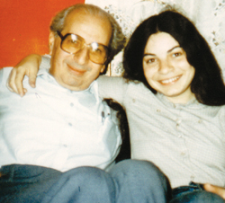
| Erwin and Monica Friedlander in 1990 |
Physics and music were his passion. His family was his life. But maybe his biggest passion of all was life itself. No one lived it more fully and made each minute count more than my father. A long time member of the Nuclear Science Division, he died on Jan. 22.
He taught me about Bach and the Beatles, about quarks and chaos and probabilities, about the origin of words, about history and literature. From him I learned how to cook spaghetti, drive a car, and how to laugh at the world and myself. But more than anything, he taught me how to survive, a lesson I most need to remember now that he can teach me no more.
I was a child living half a world away in Romania when I first heard about Lawrence and his wondrous accelerator in America. I had no clue what an accelerator was, but knew it had something to do with the stacks of nuclear emulsions that my father and “his girls” scanned under those bulky microscopes. His girls were the two dozen scanners who worked in the cosmic rays laboratory he founded in Bucharest more than 40 years ago.
One of the pioneers in using emulsions for cosmic ray research, my father was equally passionate about statistics, and had an uncanny ability to use statistical analysis to extract significant information from small samples of data. During the last year of his life he planned to write a text on statistics for experimentalists, perhaps the only major project he never saw to fruition.
His interests ranged from models of multiple particle production in high-energy collisions to coherence effects in heavy-ion collisions and quark-gluon plasmas. He published more than 250 papers and worked closely with such Lab notables as Glenn Seaborg and Ed McMillan, among many — as well as with collaborators throughout the world. He was a member of the Romanian Academy of Sciences and a recipient of the Alexander von Humboldt fellowship.
But perhaps more than anything my father was a survivor in the most humane sense of the word. Not only did he overcome extraordinary hardships, but always emerged with an enduring faith in the goodness of men.
He was traumatized by war, but never embittered. He survived labor camp under Nazi occupation, imprisonment under Stalinism, and haras-sment under Communism. In 1975 he endured temporary separation from his family when he sought freedom and defected to the West. Here he started a new life at 51 with exactly $10 in his pocket. And then he survived the cruelest trick of fate yet, when his own body began to turn against him.
But he never gave in or gave up — not when he was wheeled in for surgery and cracked jokes with the doctors; not when he was robbed of much of his eyesight yet continued his work; not when he was told he’d never walk again, and walk again he did. In 2002, five months after doctors considered ending his life, he and my mother celebrated their 50th wedding anniversary. And another two years later he finished his memoirs about science under Communism.
 |
|
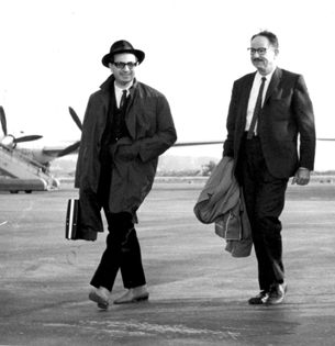
| Erwin Friedlander (left) and former Lab director Ed McMillan arrive in Warsaw, Poland, for a physics conference in 1967. | |
Oh, how I often envied him! Aside from his receding hairline, the thing I teased him most about was how he kept all his great talents to himself — genetically speaking, that is. Science aside, he played the piano like a pro, could dance to every rhythm, and spoke seven languages fluently. Meanwhile I couldn’t make heads or tails of a differential equation. But what he gave me was more precious than any of the above: he opened my eyes to the wonders of the world, and taught me how to never stop to wonder.
His joy of discovery is something my father shared with everyone he met — from his students in half a dozen countries to his cardiologist who cried openly when he recounted his first encounter with my father. Two days before his death, I told him about the Quark Matter conference, then being held in Oakland. His eyes lit up, as he had been among the first to point out that important information about quark matter could be obtained from particle reaction data. The following week, former Nuclear Science Division director Lee Schroeder referred specifically to that conference as he recalled my father’s contribution to science.
“With his strong background in statistical techniques as applied to data analysis, he helped characterize and capture our early understanding of the collision processes between two energetic nuclei. This was an essential step that the field needed to take before delving deeper into the possibilities of the creation and detection of new states of nuclear matter. As such, the recent meeting of the relativistic nuclear collision community at Quark Matter ’04 represents a legacy of Erwin Friedlander’s work.”
My father’s legacy, however, extends beyond science. Few things were more meaningful to him than his intense involvement with the human rights organization SOS — Scientists for Sakharov, Orlov and Sharanski. Founded at Berkeley Lab in 1978, the international group successfully sought freedom for scientists imprisoned in the former Soviet Union.
My father’s concern for those left behind the one-time Iron
Curtain continued through his retirement, when his loyalty both to
his research and to the laboratory he founded in Romania led to a
unique legacy, which ties into the very fabric of Berkeley Lab history.
In the days after the fall of Communism in Romania, my father set
up a collaborative experiment sending the last beam runs from the
Bevatron to Bucharest. Utilizing the infrastructure he had set up
decades earlier in Romania, he and his collaborators were able to
obtain what was probably the world’s first full-stack emulsion
scan in the world. The collaboration helped “his girls”
make a living, and in the process produced a unique database of experimental
data that will serve science into the future.
My father always quoted Einstein’s famous words about God not playing dice with the universe. In that spirit he never stopped trying to find rhyme and reason to the mysteries of Nature. How interesting that of all the wonders of the world, he was most passionate about the goings on at the tiniest scale known to mankind — the subatomic world. Yet his biggest legacy may be at a scale that can’t be measured or examined under a microscope: the human spirit.
The author is editor of the View.
A memorial for Erwin M. Friedlander will be announced. Plans are also underway to start a scholarship fund in his name. For more information, email MSFriedlander@lbl.gov.
Building ‘Ethical Climate’ Key to Institutional Success, Says Expert
BY CHRIS JONES
 |
|
| Al Erisman | |
“How should we think about ethics?” This was the central question posed by Al Erisman during his talk, “Nine Good Reasons to Be Ethical at the Lab,” recently hosted by Computing Sciences.
Erisman is the director of the Institute for Business, Technology, and Ethics, a nonprofit organization that explores ethical issues created by technology in business and institutions. His lecture at the Lab was a primer on the different ways ethical issues arise in today’s fast-paced, bottom-line work environment.
At a publicly funded institution such as the Berkeley Lab, ethical breaches can affect everything from future funding to relationships and research opportunities with other institutions.
“For a lab or any organization, in creating an ethical climate that goes beyond compliance to something that has values and culture, and is innovative and exciting, there is a financial payoff,” he said. Still, ethical problems will inevitably arise, and when they do it’s the organization’s response that ultimatelymakes the difference and sets a future course, he said.
Erisman’s nine good reasons to be ethical include:
- legal problems are decreased;
- increased regulation is deterred;
- public acceptance increases
- investor/stakeholder confidence is
maintained; - trust from partners increases;
- customer loyalty continues;
- employee performance is boosted;
- personal pride is instilled;
- it’s the right thing to do.
As can be seen in recent headlines, some of the more serious ramifications of ethical misconduct include jail time, fines, and career loss. But Erisman stressed the importance of strong principles and trust in building a healthy work environment, where employees can collaborate freely and are motivated to work hard toward common goals. Promoting humility and collaboration can go a long way toward building a healthy organization, he explained, while finger-pointing and not “walking the talk” are common pitfalls.
There are a number of underly-ing forces that exert pressure on today’s business and research institutions, he said, such as the speed of technology, a focus on short-term goals, and old-fashioned greed. All of these present difficult ethical considerations, particularly in situations involving technological research, where specific rules may not even exist. Noting the recent scandals at high-profile companies like Enron, Tyco, and WorldCom, Erisman said that executives and higher-ups sometimes believe they are above the law — and this is where things start to go awry.
In closing, Erisman explained that ethics should be part of the core mission at any institution and a component of everyday work, hiring and training. When one person’s ethical breach causes a change in regulatory policies, he said, everyone suffers, and it becomes an endless and complicated process to repair the damage.
“If you have the right principles, you can avoid trouble,” said Erisman. “And if it isn’t deeply rooted, it will fail in tough times.” For more information, visit www.ethix.org/.
Berkeley Lab View
Reid Edwards, Public Affairs Department head
Ron Kolb, Communications Department head
EDITOR
Monica Friedlander, 495-2248,
msfriedlander@lbl.gov
STAFF WRITERS
Lyn Hunter, 486-4698
Dan Krotz, 486-4019
Paul Preuss, 486-6249
Lynn Yarris, 486-5375
CONTRIBUTING WRITERS
Jon Bashor, 486-5849
Allan Chen, 486-4210
FLEA MARKET
486-5771, fleamarket@lbl.gov
Design & Illustration
Caitlin Youngquist, 486-4020
TEID Creative Services
Berkeley Lab
Communications Department
MS 65, One Cyclotron Road, Berkeley CA 94720
(510) 486-5771
Fax: (510) 486-6641
Berkeley Lab is managed by the University of California for the
U.S. Department of Energy.
Online Version
The full text and photographs of each edition of The View, as well as the Currents archive going back to 1994, are published online on the Berkeley Lab website under “Publications” in the A-Z Index. The site allows users to do searches of past articles.
Flea Market
- AUTOS & SUPPLIES
- 03 TOYOTA COROLLA CE, 8K mi, warranty, maint rec, exc cond, at,
airbags, ac, am/fm/cd, $11,450, Saito, 643-3374
02 HONDA CIVIC LX, 4 dr sedan, at, ac, alarm, fact warr, exc cond, 18.5K mi, wht, orig owner, $11,500, neg, Liem, (925)945-0243
99 HONDA ACCORD EX, exc cond, 4 dr, 4 cyl,at, ac, moonrf, $9,200 b/o, Cathy, X4067, (707) 864-9451
99 FORD WINDSTAR LX minivan, V6/3.8L, 72K mi, cruise, ABS, alloy whls, Karr sec syst, $7,600, KBB priv price $8,625, Keiji, X5850, 525-3790
HOUSING- BERKELEY HILLS, 1 bdrm/1 bth apt, fully furn, beautiful, spacious,
recently remod, w-w carpet, patio, walk to shops/public trans, nonsmoker,
quiet /safe area, $1,190/mo, Helga, 524-8308, Ivankash@hotmail.com
BERKELEY HILLS, attractive, part furn craftsman home w/ north bay view, quiet, woodsy neighbrhd, 2 bdrms/1bth, lge liv rm w/ fp, beam ceiling, hardwd flr, remod kitchen w/ new appliances, patio, garage, walking dist to UC/Lab, $2,400 mo, 6-mo renewable lease, neg, Susan, 848-1335, BeckHen@aol.com
BERKELEY, 1 bl to UCB, furn 1 bdrm apt, hardwd flrs, $1,575 incl PC, DSL & some util, Paul, X7363, 845-5959, jin.young@juno.com
BERKELEY, 3 mo only 2/1-4/1, split level, part furn studio downst from our home, priv entr, small garden, part view of SF & bay, gas range, refrig & heater, str park, nr Lawrence Hall/Lab/pub trans, $600/mo + occas pet/garden-sitting, incl gas, elec, water, garbage & high sp cable internet, $1,000 move-in cost incl 1st mo rent + $400 sec dep, refer & or credit rep req, Kathy or John, 841-7875, John.McCarthy@Comcast.net
BERKELEY, Carleton/Grant, nr BART/ shops/Lab shuttle, close to LBNL, newly renov 2 bdrm apt, ground flr of 2- story Victorian house, sunny southern exposure, front garden, w&d, custom tile flrs, no smok/pets, $1,400/mo incl part utils, avail Mar 1, Richard or Hope, 845-1723
CENTRAL BERKELEY, nice furn rms, kitchen, laundry, PC, DSL, hardwd flrs, brkfst, nr campus/shops, $950/mo include everything, Paul, X7363, 845-5959, jin.young@juno.com,
KENSINGTON, furn rm avail for vis scholar during winter/spring term, kitchen access, $500/mo, Ruth, 526-2007
KENSINGTON, quiet 2 bdrm/1.5 bth home avail to lease 4/1 - 7/1, full furn, lrg yrd, bay view, wooden flrs, w&d, parking, more, close to Kensington Village shopping & bus, 3 mi to UC, small car avail to lease, $2,000/mo + dep, non-smoker, Todd, 642-6090 days, 559-3951 eve
NORTH BERKELEY HILLS, studio, $750 rent, unfurn, $750 dep, carpet & Spanish tile, garden exposure, priv entr, kitchenette, laundry, water & garbage incl, single perso, non-smoker, no wheel chair access, str parking, Larry, 524-7610, morrison_ l@netzero.net
NORTH OAKLAND, 1 bdrm flat, upper unit in Victorian duplex, $895, nice unit w/ lots of light, space & privacy, remod kitchen, quiet, tree-lined resid str, walk to Ashby BART, nr Emeryville, Berber carpet & tile, w&d, 1 bl from Berkeley border, 1st + last + $1,000 dep, 877 61st @ Market, avail 2/13, katherinebettis@ yahoo.com, 697-1860
NORTH OAKLAND, 2 bdrm backyrd cottage, $1,300, quiet, tree lined resid str, remod kitchen, privacy, walk to Ashby BART, 1 bl from Berkeley border, w&d, yrd, 1st + last + $1,000 dep, 877 61st @ Market, avail 2/13, 1 dog OK, katherinebettis@ yahoo.com, 697-1860
SAN PABLO, 2 bd house + 1x room + 1 bd studio, $2,100, 5 min to the I-80, 20 min to Berkeley, Carmen, (650) 743-0038, Ccausso@yahoo.com
HOUSING WANTED- FEMALE seeks house to share in Alameda/ Orinda/Lafayette or other small, peaceful town in the area, non-smoking, quiet & responsible person, rent outright or work/trade, Christina, 865-0863, clonzisero@hotmail.com
MISC FOR SALE- BED full size, matt & box spring, looks new, clean $60: twin
size bed, matt & box spring, w/ frame, looks new, clean $40;
Trek mntn bike 20”, 18-sp, good cond, $20; roller skates for
girls, sizes 11 & 13, free; Amana refrig, 19 cu ft white, 3-yrold,
$200; Whirlpool washer, 6 cycles, good cond, $70, Chris, X6901
NEW TWIN BOXSPRING w/ sep allergycontrol cover, never used, b/o, Derek, X5739, 482-1420
CALIFORNIA KING, foundation & frame, new cond, $50, Tracy, X7668
DINING TABLE, seats 8, purch from Berkeley Restoration for $1,500, 83.5x40, solid hrdwd, reddish brwn, exc cond, $450/bo; couch. 80” long w/ 2 reclining sect, offwhite w/pattern, high back, good looking, very comf, exc cond, $300 /bo, sofa futon bed, full blk wd frame, cover is blk trim w/col pattern, exc cond, $150/bo, photos on request, Jiamin, X6004, 841-7556
PANASONIC 20” TV w/ stereo & fm, $98; Samsung progressive scan DVD/CDRRW/ MP3/VCR player $85, Liem (925) 945-0243
PANASONIC TV 25” color CTG-2530, video & audio jacks, quartz tuning, modern wood cabinet, exc picture, exc cond, $75; TV swivel base, 24”x15”, $13, Ron, X4410, 276-8079
TREK 720 HYBRID, 21” frame, lge city bike, almost new, $150/ bo, willing to trade for road bik, Jim, X6048
LASERDISC, Northern Exposure, whole first season. $30 (will negotiate), Eva, X2542
FREE- TREADMILL, Vitamaster Vita Trainer, programmable sp/incline, Jiamin, X6004, 841-7556
WANTED- CARPOOL from Alameda or Oakland to Lab, number of days as convenient
for driver, will contribute gas money, Christina, X4615, 865-0863
USED CAR, Honda or Toyota, less than 10 years old, Joe, X7284 -
VACATION - LAKE TAHOE, 3 bdrm, 2.5 bth house, quiet, sunny, skiing nearby, views of water & mountains, $195/night, 2 nights min, Bob, (925) 945-9345
Flea Market Policy
Submissions must include name, affiliation, extension, and home phone. Ads must be submitted in writing (e-mail: fleamarket@lbl.gov, fax: X6641,) or mailed/delivered to Bldg. 65.
Ads run one issue only unless resubmitted, and are repeated only as space permits. The submission deadline for the Feb. 20 issue is Friday, Feb. 13.
Regional Science, Industry Leaders Chart Future Of Nanoscience in Bay Area
BY DAN KROTZ
About an hour after the Molecular Foundry’s groundbreaking, several Bay Area scientists and industry leaders asked, “why here, why now, and what’s needed to shepherd nanoscience from research labs to everyday use?” The forum was sponsored by the Bay Area Science and Innovation Consortium.
Sean Randolph of the Bay Area Economic Forum kicked off the discussion. “To ensure that nanoscience research also flourishes here, we need to encourage collaborations and public- private partnerships.”
Randolph believes the Bay Area’s myriad resources could help launch the next technological revolution as long as collaborations are forged among different scientific disciplines and institutions.
“This is the center for major innovation,” said Juri
Matisoo, vice president of technology for the Semicon-ductor Industry
Association. “It is very hard to find a place like the Bay Area
with so many universities, government labs, private labs, and entrepreneurs.”
“This area fosters independent thinking,” added Paul Alivisatos,
director of the Molecular Foundry. “But nanoscience problems
are large, and progress will require a great deal of cooperation.”
Carolyn Bertozzi, director of the Molecular Foundry’s biological nano-structures facility, offered a roadmap toward such collaboration. “We need to break down the language barriers between the disciplines,” said Bertozzi. “We need to ask questions like: What can a synthetic chemist skilled at making molecules bring to the semiconductor manufacturing arena?”
Another panelist believes the Molecular Foundry, which will attract a diverse range of scientists from across the nation, will also foster interdisciplinary cooperation.
“The Bay area is the land of opportunity,” said Hans Coufal, director of science and technology at IBM Almaden Research Center. “But we are not world leaders because we have not yet torn down the walls. We have to learn to work more closely together, and the Molecular Foundry will be a catalyst for this cooperation.”
As for translating nanoscience research to real-world nanotechnology, Stan Williams, senior fellow and director of quantum science research at HP Labs, cautioned that success won’t be easy or quick. But it is possible thanks to new facilities like the Molecular Foundry.
“The Molecular Foundry is the next step in the chain from research to technology,” Williams said.