Although much larger than the nanoscale, micromachines produce nanoeffects. "The laws of physics don't change as you go to smaller structures, of course, but as they scale down, their interaction changes," Jackson says.
Nanoeffects are important, for example, in the kind of microchannel arrays used for gene sequencing and other biological analyses. "Fluid flowing through a wide canal is only grossly affected by the containing walls, but in a microchannel -a thin capillary-sidewall chemistry, plus electrofluidic and osmotic effects, may dominate."
"The driving application" of micromachine technology these days, says Jackson, is the race to build optical switchers for fiber networks. Light waves-typically a few hundred nanometers in length-carry gigabytes of data, but the flow is interrupted when light has to be converted to electrons for processing and switching, then converted back. "A big electronic router costs tens of millions of dollars, so there's an economic push to go to all-optical switchers."
|
|
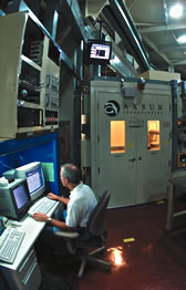
| AXSUN Technologies has sponsored the construction of an ALS beamline dedicated to LIGA, a lithography process for machining microdevices. | |
AXSUN Technologies, based in Massachusetts, recently sponsored the construction of a new LIGA beamline at the ALS to build subsystems of optical switchers, such as lenslets and flippable micromirror arrays, for dividing and steering streams of data-carrying photons. "It's almost like a free beamline for the scientific community," Jackson says, because it will often be available for noncommercial work.
To tap into this new world of startling possibilities, researchers must start with the palpable. Says Jackson, "To study nanophenomena, you need microtools."
NANOWRITING
Electrons, with effective wavelengths two orders of magnitude shorter than hard x-rays, can expose nanoscale features directly.
"In the mid-1990s we saw the need for advanced electron-beam lithographic capability," says Erik Anderson, head of CXRO's Nanowriter facility, "and we were at the right place at the right time." The Defense Advanced Research Projects Agency supported the acquisition of the world's first Leica Microsytems nonprototype Nanowriter, whose electron beam can directly expose a resist-coated substrate on a moving surface controlled by laser interferometry.
|
|
|
| The Nanowriter is an ultrahigh resolution lithography machine that can generate an electron beam at energies up to 100,000 volts with a diameter of five nanometers or less. | |
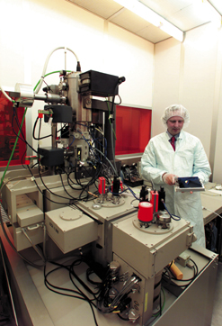
Hardware includes a 100-kilovolt power supply that accelerates energetic electrons off the Nanowriter's thermal-field-emission gun and an optics column that can focus the beam to a width of from 5 to 2.5 nanometers. Anderson and his colleagues added custom electronics and software to control the operation of the system, such as the movement of the stage through laser feedback; they also built a unique pattern generator that controls the position of the beam.
The Nanowriter can create quantum "dot" electronics, magnetic thin-film devices, and structures such as Gabor Somorjai's catalytic nanoarrays. To meet the demands of Moore's "law," which dictates a doubling in the electronic devices per chip every 18 months, the continually-improving Nanowriter draws ever-finer patterns for ever-more-densely-packed circuits. An important feature is the machine's ability to "stitch" together adjacent areas of circuitry with nano-accuracy.
Meanwhile the Nanowriter keeps busy making zone plates for experiments at the ALS. Concentric rings, the smallest of them as small as 25 nanometers wide, are fabricated from massive materials like gold, producing a wide variety of microscopic planar structures to focus x-rays that would pass unaffected through conventional lenses.
The increased demand for nanodevices of every description means that "we collaborate with a wide community, working together to achieve the smallest features," says Anderson. "It's a never-ending challenge."
MAKING THE MOLECULES DANCE
When a small voltage is applied, a current flows between the tip of a scanning tunneling microscope (TEM) and the electrons surrounding the atoms on a nearby surface. Scanning back and forth in raster fashion while adjusting the voltage to keep the current uniform (or vice versa), the TEM graphs the surface's ups and downs to create a topographical image, atom by atom.
"Scanning tunneling microscopes are sensitive enough to follow atomic profiles-that's the easy part," says Miquel Salmeron of the Materials Sciences Division. "Our goal is to study the behavior of individual atoms and molecules."
Among many other systems, Salmeron and his colleagues have studied acetylene in such detail that they have learned just how much energy it requires to nudge these tiny molecules-two atoms of carbon and two of hydrogen-from one orientation to another as they nestle in the lattice of a palladium surface.
At normal temperatures an atom is in constant frenetic motion and can't be imaged. "By immersing the TEM in liquid helium, we immobilize the atom," Salmeron says. "We send electricity through the tip to confirm that we have it; once we've found it, we can move it around."
How to do this "is not written anywhere," he says, "but for each particular atom or molecule we have our tricks. We can shoot electrons at it. Or kick it into rotation. Or it may jump to the tip. If it's a molecule, we can smash it."
Salmeron's interest in catalysis led to his studies of acetylene on palladium, which selectively catalyzes benzene (six atoms of carbon and six of hydrogen) from three acetylene molecules. Attempts to trimerize the acetylene molecules by nudging them with the TEM tip have not succeeded, but Salmeron has succeeded in making the molecules rotate. "It takes just one electron to make the acetylene molecule rotate 120 degrees among three atoms of palladium." Changes in position reflect the molecule's attempts to accomodate extra charge. Repeated kicks make the molecule spin.
|
|
| Nestled among the atoms on a palladium surface, acetylene molecules spin in increments of 120 degrees. |
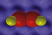
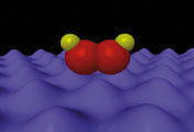
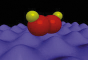
A remarkable set of movies shows acetylene in action: the molecules look like little Mickey Mouse heads spinning merrily on the palladium surface-the two carbon atoms form a single white blob with hydrogen "ears," corresponding to what Salmeron calls "black holes" (on the web at http://stm.lbl.gov/research/cryostm/c2h2/).
"Most of what we call nanotechnology involves hundreds or thousands of atoms," says Salmeron, "but in a nanometer there's enough room for three atoms. If we are going to achieve real nanotechnology, we are going to have to learn how to put atoms together one at a time." - end -
| < Research Review | Top ^ | Next > |