
|
|

| "Nanocrystals
are particularly attractive as building blocks for larger structures
because it's possible - even easy - to prepare nanocrystals that are
highly perfect." So says Paul Alivisatos, a chemist who holds a joint appointment with Berkeley Lab's Materials Sciences Division (MSD) and with the Chemistry Department of the University of California at Berkeley. Alivisatos is one of the leading lights in the burgeoning field of nano-sized semiconductor crystals. |
|
|
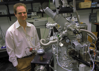 |
| Chemist Paul Alivisatos is a leader in the development of nano-sized crystals that could serve as building blocks for electronic devices a few billionths of a meter in size. | |
Nanocrystals are aggregates of anywhere from a few hundred to tens of thousands of atoms that combine into a crystalline form of matter known as a "cluster." Typically around ten nanometers in diameter, nanocrystals are larger than molecules but smaller than bulk solids and therefore frequently exhibit physical and chemical properties somewhere in between. Given that a nanocrystal is virtually all surface and no interior, its properties can vary considerably as the crystal grows in size.
"By precisely controlling a nanocrystal's size and surface, its properties can be tuned," Alivisatos says. "You can tune the bandgap, you can tune how it conducts charge, you can change what crystal structure it resides in, you can even change its melting temperature."
Growing flawless nanocrystals is relatively easy because their length of scale is so small there's simply not enough time during the growth process to introduce defects. This same tiny length of scale, however, makes controlling the size and surface of nanocrystals a tremendous challenge. During the past decade, Alivisatos and his research group have been growing nanocrystals out of semiconductor powders and exploring various ways of altering growth conditions as a means of meeting this challenge.
|
|
|
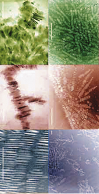
| The images above show the variety of shapes and sizes that nanocrystals can be made to assume. The rod-shaped nanocrystals to the far left can be stacked for possible use in LEDs, while the tetrapod to the far right should be handy for wiring nano-sized devices. | |
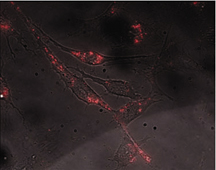
One of Alivisatos' first big breakthroughs came when he and collaborator Shimon Weiss discovered that spherical nanocrystals made from a core of cadmium selenide inside a shell of cadmium sulfide could, depending upon their size, be made to emit multiple colors of light. This opened the door to a number of potential applications, including the use of these spherical core-shell nanocrystals as highly effective fluorescent labels for the study of biological materials. In fluorescent labeling, markers, usually antibodies that attach themselves to specific proteins, are tagged with dye molecules that fluoresce or emit a specific color of light when stimulated by photons, usually from a confocal microscope.
"Sometimes in order to fully characterize a biological sample, a population of cells for example, you need to look at combinations of markers," says Alivisatos. Such measurements require multiple-color light emissions which are difficult to obtain with conventional dye molecules.
Alivisatos and his colleagues grow their nanocrystals by injecting semiconductor powders into hot, soap-like films called surfactants. In their recent work, they've been growing their crystals in a mixture of two surfactants, one called TOPO and one called HPA, each of which reacts with the semiconductor powders in a slightly different manner. The result has added an entire new dimension to nanocrystal production - literally.
In March of last year, Alivisatos and his group made news when they announced that they had made two-dimensional cadmium selenide nanocrystals that were shaped like rods. Prior to this, the nanocrystals that had been reported had all been dot-like spheres. Demonstrating the ability to grow semiconductor nanocrystals into two-dimensional rods not only paves the way for a slew of new potential applications, it also proves that controlling crystal growth is the key to controlling shape as well as size.
"It was the first time anyone had really gotten control of semiconductor nanocrystal growth," Alivisatos said. "By controlling the kinetics of crystal growth we were able to select the size but vary the shapes of our crystals."
Although the precise mechanism is unknown, Alivisatos suspects that the interaction of the cadmium and selenium atoms with the two different surfactants causes each crystal to grow in only one direction. Consequently, maintaining a relatively fast rate of growth in the right mix of surfactants induces crystals of a selected size to assume an elongated, rod-like faceted shape that maximizes the crystal surface area.
|
|
 |
Subsequent tests showed that rod-shaped nanocrystals emit light polarized along their long axis in contrast to the nonpolarized light fluoresced by the earlier cadmium selenide nanocrystal spheres. This should be highly useful in biological-tagging studies where the orientation of a marker is critical. Other tests showed that the gap between emission and absorption energies is larger for nanocrystal rods than for nanocrystal spheres. This should be an advantage for applications such light-emitting diodes (LEDs) where the reabsorption of light can be a problem.
"We've also shown that multiple nanorods can be packed and aligned, another advantage for both LEDs and for the use of these rods in photovoltaic cells."
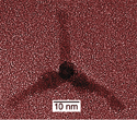
More recently, Alivisatos and his group have learned to manipulate the conditions and rate of crystal growth to the point where they have obtained semiconductor nanocrystals in the shape of tear drops, arrowheads, and even four-armed tetrapods. While these exotic shapes have no immediate application, they expand the possible things that might be built from nanocrystal blocks in the future. For example, when the tetrapod nanocrystals are dropped onto a surface they always land on three arms with the fourth arm pointing straight up. This should be a handy feature for the wiring of nanosized electronic devices.
First, however, scientists will have to learn how to assemble nanocrystals into larger, more complex structures. One idea now being pursued by Alivisatos and his group-first proposed by former Berkeley Lab researchers Peter Schultz and Paul McEuen-is to ride on the back of nature by using DNA as a template.
"In a sense, what we now have is the ability to make all the little building blocks, but we lack the chemistry that tells these blocks where they should all go," Alivisatos says. "It's possible that DNA could be used to direct the assembly of nanocrystals into arbitrary patterns of enormous complexity."
|
|
|
In the familiar "twisted ladder" image of DNA, two strands of phosphate and ribose sugar molecules are joined by "rungs" made up of a connecting pair of nitrogenous compounds called "bases." There are four types of bases-adenine (A), cytosine (C), guanine (G), and thymine (T)-and A always pairs with T, and G always connects with C. Alivisatos and his colleagues capitalize on this highly specific architectural program by using "linker" molecules to attach segments of single-stranded DNA up to 100 bases in length (about 33 nanometers) to crystals of gold measuring 5 to 10 nanometers across. When these nanocrystal/DNA "conjugates" are mixed with other segments of single-stranded DNA containing base sequences that complement the sequences of the DNA in the conjugates, the complementary bases recognize one another and pair off to form double-stranded DNA. In this manner, DNA serves as a template for creating nanocrystal molecules.
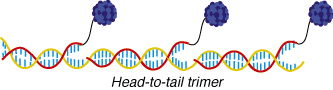 |
| DNA is being used as a template for assembling nanocrystals into macromolecules. Here nanocrystals of gold attached to a single strand of DNA are brought together into a desired alignment as the DNA's double-helix is formed. (Illustration by Meg Holm) |
Says Alivisatos, "In the strategy we're employing, the binding of DNA to the gold nanocrystals is a statistical process. By adjusting the ratio of DNA to nanocrystal we can control the average number of DNA strands per conjugate particle."
What has been needed is a way to separate and isolate conjugates according to size. Alivisatos and his colleagues have recently accomplished this using the "gel electrophoresis" technology that is a standard tool in biology for separating different lengths of DNA fragments. By placing their nanocrystal/ DNA conjugates in a porous gel under an electric field, they were able to separate and isolate gold nanocrystals attached to anywhere from one to five segments of single-stranded DNA.
 |
|
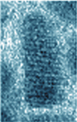
| Cadmium selenide nanocrystals were used to create this fluorescent microscopic image of living 3T3 fibroblast cells. These and other semiconductor nanocrystals could supplement dye-molecules as fluorescent labels for the study of biological materials. | |
"We demonstrated that the shift in particle mobility (in the electrified gel) due to the DNA attachment can be used to produce nanocrystal/ DNA conjugates with a well-defined number of DNA strands," Alivisatos says.
Proof that the information contained within DNA can be harnessed for the spatial patterning of semiconductor nanocrystals holds great promise for their use as nanotechnology building blocks. Although the assemblies so far have been relatively simple, the indication is that nanocrystal/DNA conjugates could be used to make structures and devices corresponding in size and complexity to the semiconductor circuits produced today using lithography.
"We've shown that we can use organic chemistry to direct the assembly of inorganic crystals," Alivisatos says. "It's a first step in transferring DNA from the biological to the material world."
| < Research Review | Top ^ | Next > |