|
SCIENCE ON THE SURFACE
PART TWO |
 |
|
SCIENCE ON THE SURFACE
PART TWO |
|
The surface science experimental station that has been set up by Fadley and his colleagues is presently located on ALS beamline 9.3.2, a bend-magnet beamline that produces photons whose energies can be varied between 30 and 1500 electron volts in energy (virtually the full range of energy that is of interest in photoelectron studies)."Being able to tune the radiation energy over this broad a range permits the study of both the inner "core" as well as the outer "valence" electrons of all elements," Fadley says. "Furthermore, we can select conditions for which the photoelectron signals are strongest and most surface-sensitive." The light from the ALS is so bright that it should be possible in the near future to measure a photoelectron speed in as little as a millisecond (one thousandth of a second); with previous sources it took minutes to accumulate a spectrum.
In addition, the light on beamline 9.3.2, like all ALS radiation, is pulsed, meaning it flashes on and off like a strobe light. The pulse rates of ALS light beams can be as high as 500 million pulses per second, with each lasting only 30 to 40 picoseconds (trillionths of a second). This should eventually allow the beams to be used as a highly effective stop-action camera for recording images of surface atom dynamics.
As a final step in commissioning their experimental station and testing its capabilities, Fadley and Hussain, working with visitor Hiroshi Daimon of the Photon Factory in Japan, and Jeffrey Kortright of Berkeley Lab's Center for X-ray Optics (located in the Materials Sciences Division), successfully characterized the surface of a sample of oxidized tungsten metal. To do this, they capitalized on a phenomenon known as "circular dichroism," whereby the amount of light a material absorbs (or the number of photoelectrons it ejects) will depend upon the direction (clockwise or counterclockwise) in which the light is polarized. Circular dichroism is especially useful in the study of surfaces and interfaces of magnetic materials because it distinguishes photoelectrons on the basis of their up or down "spin" orientation. All magnetic phenomena involve unequal numbers of spin-up and spin-down electrons with a net spin pointing in one direction.
"In a magnetically-ordered environment, photoelectrons with up and down spins may not have the same energy nor scatter with equal strength from the neighboring atoms," says Fadley. "We can use these differences to measure magnetism in the vicinity of each type of atom in a sample, even in non-magnetic atoms that may have magnetic atoms nearby."
The proof-of-principle experiment conducted by Fadley, Hussain, Daimon, and Kortright showed that strong circular dichroism effects arose even in the non-magnetic tungsten atoms which were present in both the oxide and metal surfaces. This, Fadley says, demonstrated that circular dichroism can be used to study non-magnetic as well as magnetic materials.
Measuring the degree of circular dichroism displayed by a material requires light that is circularly polarized. This capability was added to Fadley's experimental station with the installation of a unique optical system on beamline 9.3.2. After light is extracted from the ALS storage ring and sent into beamlines, it is directed to experimental stations by means of metal-coated mirrors and optical devices. Before it arrives at an experimental station, the light is passed through a "monochromator," a device that employs a combination of slits and gratings to disperse photons so that scientists can select the desired energy for their specific research purposes. The monochromator used by Fadley and Hussain is equipped with an additional moveable entrance slit that enables them to vary the polarization of their light from linear to circular. The performance of this unique moveable slit was characterized using a special polarimeter developed by Kortright.
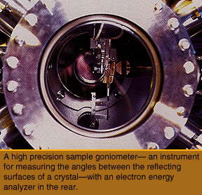
"Our photoelectron spectrometer at the ALS is also moveable," says Fadley. "It can be rotated through a 60 degree angle to allow us to vary the angle between the incident light and the outgoing photoelectron, or to keep the angle between the sample surface and the photoelectron fixed as we vary the angle of incidence of the light on the surface."
This mobility, he says, will allow him and his research team to add other dimensions to their experiments, including the ability to look selectively at interfaces buried just below the surface.
Through the combination of high resolution in both energy and photoelectron emission angles, Fadley's experimental station will enable researchers to obtain detailed information on what types of atoms are present on a surface, how many there are of each type and how they are arranged in space. They will also be able to identify the chemical or magnetic states of these atoms.
"In some cases, we will even be able to produce three-dimensional images of these atoms," says Fadley.
By treating the outgoing photoelectron wave as a reference wave and analyzing the interference patterns created with waves scattered from other atoms, it is possible, he says, to make a photoelectron hologram. With enough holographic data, true three-dimensional images of the neighbors around selected individual atoms can be produced, even if those atoms are attached to other atoms as part of a surface molecule or other nanostructure.
"Being able to characterize surfaces and interfaces in such detail will be a major advantage as we try to fabricate the next generation of nanoscale semiconductor or magnetic storage devices," says Fadley.
To his world-class experimental station, Fadley, again working closely with Hussain, will soon add a scanning tunneling microscope (STM), an instrument that can be used to map the atomic topography of a surface. Linking advanced PES/PED and STM capabilities within a single ultrahigh vacuum system (a first which Fadley already has accomplished in a bench-top experiment at Berkeley) will provide highly complementary information on the changes that atomic structures undergo during surface chemical reactions.
Another significant addition coming soon to this experimental station will be improved detectors for capturing photoelectrons. Although the station already has what Fadley describes as "a very good commercial detector" he says the data that can be extracted as a result of the unprecedented brightness of the ALS is often overwhelming.
"Without much faster detectors, it is already necessary in many experiments to artificially reduce the brightness of the ALS light in order to avoid detector saturation," he says.
To this end, Fadley and Hussain, together with engineers Joe Katz and Jorge Zaninovich, and teams from Berkeley Lab's Engineering and Physics divisions, are working on a "next generation" photoelectron detector. This high-speed multichannel detection system will collect data about 10,000 times faster than the commercial detector Fadley's group is currently using. Making use of integrated circuit technology originally developed at Berkeley Lab for the ill-fated Superconducting Super Collider, this new type of detector will be capable of recording a full photoelectron spectrum in a thousandth of a second, as compared to the present seconds to minutes of operational time.
"When developed, this next-generation detector should find wide use at other ALS experimental stations besides ours," says Fadley. "It should also be applicable to atomic and molecular physics and a number of other fields in addition to surface science studies. We are now working with a local company to commercialize it."
Further down the road, Fadley and Hussain plan to install a second new detector that will permit direct measurements of photo electron spin in studies of magnetic samples. This second system is being designed and built in collaboration with ALS physicist Neville Smith and with researchers at Florida State University. When both new detectors are in place, researchers will be able to use Fadley's experimental station to do PES/PED studies with unprecedented resolution, flexibility, and speed.
As a final improvement, Fadley says, his entire experimental station will be moved sometime in 1997 to an elliptically-polarized undulator beamline that is presently under construction at the ALS. This new beamline will provide photons of variable polarization at 50 to 100 times the brightness of what is currently available.
"Nanotechnology is going to increase the pressure for smaller and thinner devices; everything will have to shrink in size," says Fadley. "When you are talking about circuits whose elements are only 20 atoms thick or 20 atoms wide, the devices become quasi-two and one-dimensional objects. At that level, surfaces and interfaces dominate behavior. I think we have put together a truly unique system on a world scale for preparing and characterizing such nanomaterials."
Thirty-six years ago, Richard Feynman gave a lecture and some people laughed. Nobody is laughing now.
 |
 |
 |