|
|
| |
 |
 |
|
| |
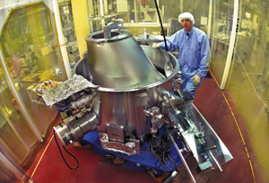
Erik Anderson, director
of the Center for X-Ray Optics, with the extreme ultraviolet
"at-wavelength" interferometer at the Advanced
Light Source. |
| |
|
The extreme-ultraviolet "at-wavelength" interferometer
at the Advanced Light Source's beamline 12.0.1 is arguably
the most accurate wavefront measuring device in the world.
Operated by the Center for X-Ray Optics (CXRO), this device
has lately morphed into a mechanism that can print semiconductor
wafers by itself.
"The interferometer is wonderful for testing optics,
but the proof of what the optics can do is in the printing,"
says CXRO's director, Erik Anderson. In its new configuration,
the interferometer delivers the printing proof.
For decades the semiconductor industry has been packing ever
smaller, ever more numerous electronic devices onto chips,
doubling density roughly every eighteen months by using photolithography.
In 1994 manufacturers began searching for ways to use even
shorter wavelengths.
Extreme ultraviolet lithography is the technique championed
by a group of companies including Intel, Motorola, Advanced
Microdevices, Micron Technology, Infineon Technologies, and
IBM, working closely with the Department of Energy's "Virtual
National Laboratory" consisting of teams from Lawrence
Berkeley, Lawrence Livermore, and Sandia National Laboratories.
Berkeley Lab's participation was spearheaded by EUV program
manager and former CXRO head David Attwood.
The wavelength chosen by the EUVL collaboration, about 13
nanometers (13 billionths of a meter), is readily absorbed
by glass lenses--indeed by all materials, including air--so
the beams must be focused by curved mirrors instead. These
are built up from dozens of layers of silicon and molybdenum,
each a few atoms thick. A small fraction of the light reaching
each layer is reflected, but the reflections constructively
interfere, adding up to some 70 percent of the total falling
on the mirror.
|
|
| |
"The interferometer
is wonderful for testing optics, but the proof of what
the optics can do is in the printing." |
|
|
To test the mirrors, an incoming beam of coherent EUV radiation
is split in two. One beam acquires the aberrations of the
optical system while the other forms a nearly perfect reference
wave. If the optics were flawless, interference between the
two beams would constitute a perfectly regular array of fringes;
in the real world, aberrations displace the fringes from their
ideal location.
A CXRO team tested two sets of four mirrors for the prototype
EUV printer built by Sandia, measuring tolerances so fine
they were less than the radius of a hydrogen atom. One set
of mirrors was used when the prototype printer went into service
in 2001. The second set was not immediately needed, so the
team modified the at-wavelength interferometer to print test
patterns from them.
The resulting device was called the SES, the "static
exposure station"--static because, unlike the full-blown
Sandia printer, it projects only a portion of a mask pattern
and exposes only part of a wafer at a time.
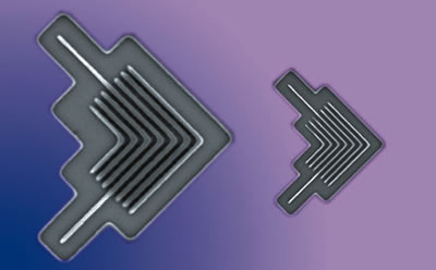
The optics performed even better than their design specified.
Mirrors designed to make features with resolution better than
100 nanometers readily created 70 nm features. By manipulating
parameters like beam angles and exposure times, the CXRO team
achieved much smaller features, with a line width just 39
nanometers wide.
|
 |
| |
 |
| |
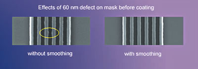
| (Top) The CXRO team programmed
defects into masks, then used coatings optimized for smoothing
to reduce the irregularities in printed features. (Above)
Researchers easily created 70 nm features on chips, as
in these "elbows." By changing parameters, they
were able to achieve much smaller features, with a line
width of just 39 nm (far right). |
|
The SES also tested ways to get rid of defects in the flat
masks, also made of multiple layers. Even the tiniest flaw
in a mask can damage a circuit printed from it, and flaws
can occur on the substrate or in any of the mask's dozens
of layers.
"If there's a defect at the bottom of all those layers,
you can't directly repair it. So the question is how to smooth
it out," Anderson says. The team used the Nanowriter,
CXRO's ultra-high-resolution electron-beam lithography machine,
to create masks with programmed defects.
The SES printed from these masks using different coatings
developed at Livermore. Anderson says, "Coatings optimized
for smoothing minimized the irregularities, like snow on grass.
With non-smooth coatings, the defects stood out like snow
on a boulder."
By printing from the newest set of optics and special test
masks, says Anderson, "we have verified the interferometry
and demonstrated the impressive capabilities of EUV lithography."
These capabilities were sufficiently impressive that in April
of 2002 Intel ordered the first production EUV stepper from
the manufacturer ASML, to be delivered in 2005. Meanwhile,
manufacturers hope to extend current photolithography techniques
to 157 nm wavelengths, making chips with line widths less
than 70 nanometers. To make anything smaller than that, EUVL
is essential.
By 2007, commercial production is expected to begin, using
an EUV stepper to manufacture chips with 18 nm gate widths
(after etch). In October 2001, manufacturers chose EUVL as
the most likely technology to be able to create chips with
gate widths only 13 nanometers wide by the year 2009.
That will be just the beginning of the next generation of
superdense integrated circuits.
-- Paul Preuss
|