|
|
|
|
 |
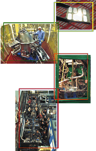
Science fiction writer Arthur C.
Clarke once noted that a thin line separates the most advanced
technologies from magic. Nowhere is that line thinner than in
the burgeoning fields of nanoscience and advanced materials,
with their promise of electronic devices shrunk down a thousand
times from today's microtechnology, and manufacturing processes
that take place at the atomic and molecular levels. This past
year, Berkeley Lab researchers worked scientific "magic"
with the fabrication of solar cells and multipurpose wires too
small to be seen even with the most powerful optical microscopes.
They also bolstered the capabilities of the Advanced Light Source,
one of the world's premier synchrotron radiation sources for
nanoscience and advanced materials research, with the addition
of new instrumentation for extreme ultraviolet light studies
and new superconducting magnets for producing high energy x-rays.
Berkeley researchers also completed their contribution to the
Spallation Neutron Source, which will be the world's premier
facility for the study of material properties through neutron
scattering. |
|
|
|
|
|
|
 |
|