At this new experimental station, Berkeley Lab researchers working with users from outside the Laboratory will be able to obtain detailed information on what types of atoms are present on a surface, how many there are of each type, and how they are arranged in space. It will also be possible to identify the chemical or magnetic states of these atoms, and in some cases to produce holographic images. The information learned will provide U.S. chip manufacturers with a big advantage in their efforts to fabricate nanoscale semiconductor and magnetic storage devices.
Nanoscale devices are so small they become two- or even one-dimensional objects-essentially nothing but surfaces and interfaces. Another critical factor in bringing nanotechnology to fruition will be a better understanding of how electrons move through materials that are less than three-dimensional. Berkeley Lab scientists studying the dynamics of electrons at surfaces made strides recently with the solution of a long-standing problem concerning the effect on the motions of electrons near a metal surface when that surface is coated with thin films of an insulating material. Making good use of new lasers that can deliver tunable pulses of light only 100 femtoseconds in duration (one femtosecond is a millionth of a billionth of a second), the scientists have been able to follow electrons as they move back and forth across the interface between a metal surface and an insulating film of molecules. They've also been able to vary the thickness of the insulating film by a single layer of molecules at a time in order to study the effects on electron movements as devices increase from two dimensions to three. What made this research possible in addition to femtosecond lasers was a technique called "two-photon photoemission" and an unusual electron time-of-flight detection scheme that gives unprecedented sensitivity and highly precise energy measurements.
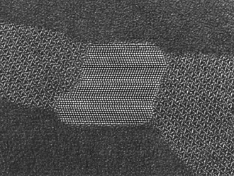
Berkeley Lab scientists this past year also successfully demonstrated the first ever catalysis on a nanometer scale. Working with UC Berkeley researchers, they modified an Atomic Force Microscope so that it functioned like an ultrafine-point pen for catalytic calligraphy. With this unique new tool, they were able to create a reaction that changed the chemical composition of the surface of a material one molecule at a time.