| science@berkeley lab | | lab a-z index | lab home |
|
|||
| Falling into the Gap Berkeley Lab Researchers Take a Critical First Step Toward Graphene Transistors |
|||||||||||||||||||||||||
| Contact: Lynn Yarris, lcyarris@lbl.gov | |||||||||||||||||||||||||
Graphene, a form of carbon whose existence was thought to be impossible until it was actually made in 2004, holds the promise of a new generation of faster, smaller, cheaper, and more durable computer chips. However, before graphene can be engineered into transistors or other electronic devices, a gap must be introduced into the electronic band structure of its two-dimensional crystal. This has now been done, by a multi-institutional collaboration under the leadership of researchers with Berkeley Lab and the University of California at Berkeley.
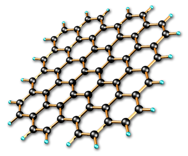
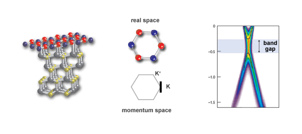
Utilizing intensely bright beams of x-rays from Berkeley Lab's Advanced Light Source (ALS), the collaborative team showed that when an epitaxial film of graphene is grown on a silicon carbide substrate, a significant energy band gap — 0.26 electron volts (eV) — is produced. "We propose that this gap is created when the graphene lattice's symmetry is broken as a result of the interaction between the graphene and the substrate, and we believe that these results highlight a promising direction for the band-gap engineering of graphene," says Alessandra Lanzara, a physicist who holds a joint appointment with Berkeley Lab's Materials Sciences Division and UC Berkeley's Physics Department. Lanzara was the principal investigator for this study. Graphene is a densely packed single layer of carbon atoms, arranged in a hexagonal pattern like a honeycomb, that forms a two-dimensional sheet; it has been described as a carbon nanotube "unrolled." Although made from graphite, the stuff of pencil leads, graphene is seen more as a diamond-in-the-rough by the electronics industry. Electrons can move ballistically through graphene even at room temperature, which means they can fly through the sheet like photons through a vacuum, undergoing none of the collisions with atoms that generate heat and limit the speed and size of silicon-based devices. Also, because carbon has the highest melting point of any element, and graphene the highest rate of thermal conductivity, it should be possible to operate electronic devices made from graphene at much higher temperatures than silicon-based devices. What graphene lacks is a gap between its valence and conduction electron-energy bands — the band gap that defines semiconductors. These bands are the energies where electrons are either tightly bound to their host atoms (valence band) or free to move through the material (conduction band). Without this semiconducting band gap, graphene sheets cannot be used in electronics technology.
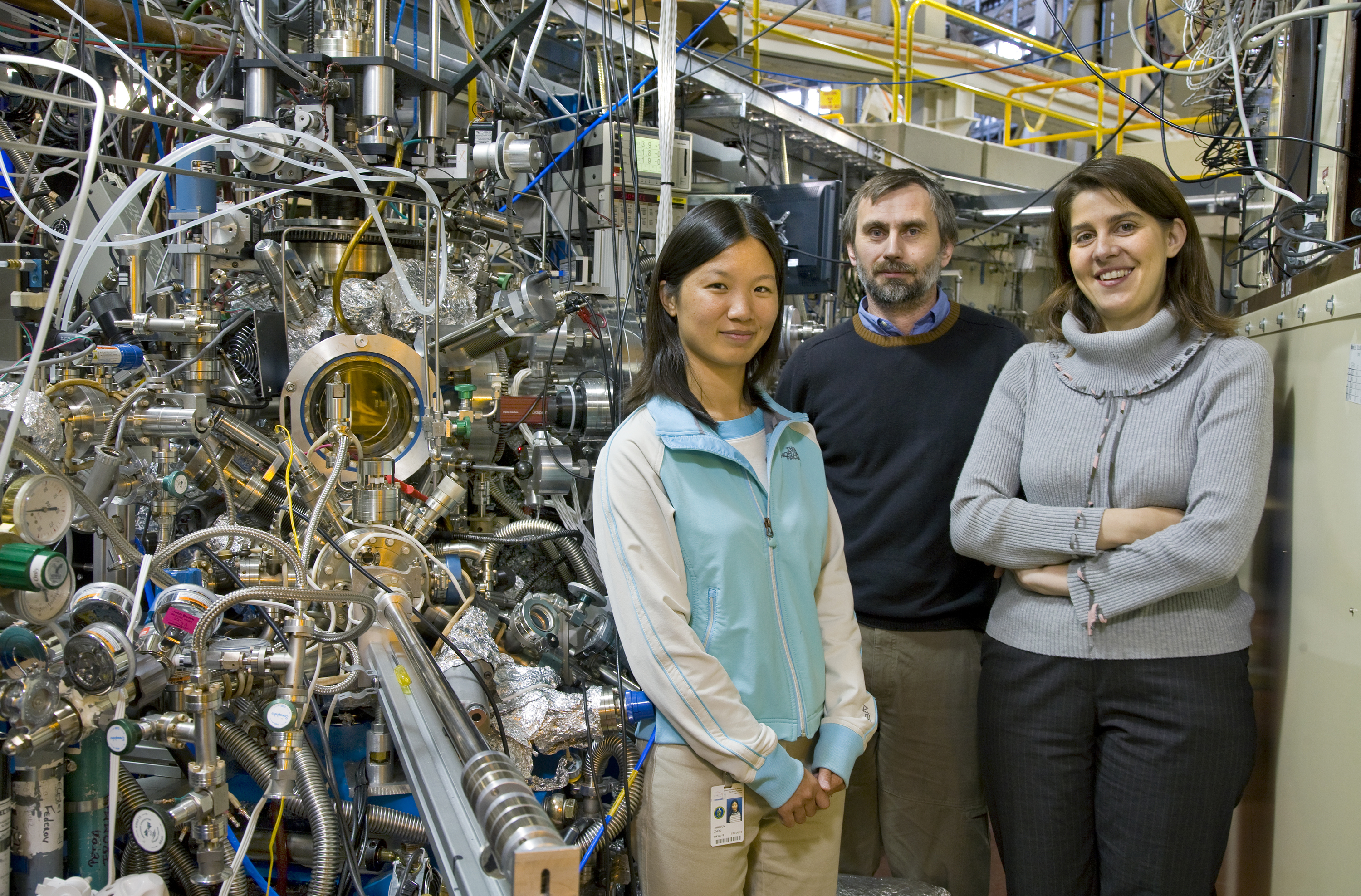
While there are several promising efforts underway to induce such a gap, through doping or through the fabrication of confined geometric structures like quantum dots or nanoribbons, Lanzara and her team have demonstrated that growing epitaxial graphene on a silicon carbide substrate could be a much easier approach, one that would work even with bulk graphene. "As far as we know, this is the first demonstration that a semiconducting band gap can be created in graphene without doping or confining the geometry," says physicist Shuyn Zhou, a member of Lanzara's research group who also holds a joint appointment with Berkeley Lab's Materials Sciences Division and UC Berkeley's Physics Department. Using a probe technique called ARPES (angle-resolved photoemission spectroscopy), plus the unique research capabilities of ALS beamlines 12.0.1 and 7.0.1, also known as the Electronic Structure Factory, Lanzara, Zhou and their colleagues obtained electronic spectra of graphene layers on a silicon carbide substrate, with unprecedented detail in the low-energy portion of the spectrum. The detail revealed a semiconductor band gap where none had been previously reported.
"The band gap decreases as sample thickness increases and eventually approaches zero when the number of graphene film layers exceeds four," says Lanzara. "Manipulating sample thickness might be one way of doing band-gap engineering, but the range of band gaps achievable is relatively small. We believe a more promising way to achieve a large range of band gaps might be through substrate engineering. Different substrates will have different potentials, and the strength of the interaction between the graphene and the substrate should lead to different band-gap sizes. Already there are predictions that a similar mechanism might open band gaps in graphene on a boron nitride substrate." Says Zhou, "On the one hand, we need the interaction between graphene and the substrate to be strong enough that a band gap will be opened up. But on the other hand the interaction cannot not be so strong that we lose the important properties of graphene. We will be investigating possible substrates for achieving this, but we have shown that epitaxial graphene devices can in principle be fabricated using the existing silicon-based technology." Although the use of epitaxial graphene as the host material for microelectronic technology remains a few miles down the road, the demonstration that electronic band gaps can be created in bulk graphene is a critical step towards that goal. Additional information
|
|||||||||||||||||||||||||
| Top | |||||||||||||||||||||||||