| science@berkeley lab | | lab a-z index | lab home |
|
|||
| When Cutting-edge Particle Detectors and Cutting-edge Consumer Products Converge A New Kind of Particle Detector Using Silicon-on-Insulator Chips |
||||||||||||||||||||
| Contact: Paul Preuss, paul_preuss@lbl.gov | ||||||||||||||||||||
Marco Battaglia of Berkeley Lab's Physics Division and UC Berkeley's Department of Physics heads the Lab's program to develop a vertex detector for the proposed International Linear Collider (ILC), in collaboration with partners at the University of Padua and the University of Turin. Peter Denes has worked with numerous detector applications, both in the Engineering Division, where he was Deputy Director for electronics, software, and instrumentation, and at the Advanced Light Source, where he recently became Deputy for Engineering. Not long ago the two men discovered they had a common interest: a new kind of electronic device called a silicon-on-insulator chip, or SOI.
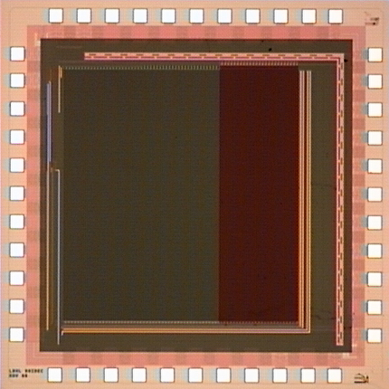
"Peter and I discovered we had parallel detector projects that could both benefit from what SOI chips had to offer," says Battaglia, "namely the potential for more and smaller pixels for better resolution, with more and faster intelligence per pixel." SOI chips are a kind of silicon sandwich, called "silicon-on-insulator" because they feature a layer of integrated-circuit electronics (CMOS transistors, complementary metal-oxide semiconductor devices fabricated in silicon), which is separated from the chip's substrate by a thin layer of silicon-oxide insulator. The substrate may be another layer of silicon, such as "high-resistivity" detector-grade silicon. Battaglia adds that one of the most attractive things about SOI technology is that it isn't some excessively expensive, arcane, one-of-a-kind science application. "SOI technology is driven by consumer electronics — cell phones, digital cameras — where the need is to squeeze everything onto one chip that can operate with low power consumption." Says Denes, "CMOS electronics drives the consumer technology. To make an SOI chip suited to the particle world, however, you need a couple of extras: a detector-grade silicon substrate on which the electronics and insulating layers rest, and added contacts between the substrate and the electronics." Battaglia and Denes note that Japan's High Energy Accelerator Research Organization, KEK, was first to come up with the idea of penetrating the insulating layer of an SOI chip with contacts between the electronics layer and a particle-detector layer. And it was KEK, working with the electronics firm OKI Electric Industry Co., Ltd., supplier of SOI chips, that organized a showcase for potential next-generation science applications of the technology. KEK invited proposals for SOI chip designs from a number of research institutions including the Japan Aerospace Exploration Agency, JAXA; Berkeley Lab; Fermilab; the University of Hawaii; and other groups. OKI — whose chief motivation, says Denes, was "an interest in clever ideas," some of which might someday find their way into commercial applications — fabricated more than a dozen of the designs all together on a single large wafer in a "multiproject run." Among the designs was Berkeley Lab's prototype "monolithic pixel sensor," designed to test the concept of a detector in which each pixel is capped with its own electronics. In the test detector, the electronics are implanted in a 40-nanometer-thick layer of silicon atop a 200-nanometer-thick insulating layer. (A nanometer is a billionth of a meter.) By contrast, the test chip's pure silicon substrate is 350 micrometers thick (a micrometer is a millionth of meter), over a thousand times thicker than the overlying electronics and insulator. KEK's idea for having the layer of CMOS electronics contact the detector layer allows the application of bias voltage to the Berkeley Lab chip's detector-grade silicon substrate. This permits the thick, highly resistive substrate to be "fully depleted" — cleared of charge — so that charge carriers created when particles strike each pixel region can travel straight through to the associated electronics with little diffusion. Spreading charge would weaken the signal; depleted regions offer much better spatial resolution and faster processing. Mounting the electronics right on top of the pixel saves precious readout time. Because particle detectors experience rapid bombardment, time is critical — unlike astronomy, for example, where the collection of light from a distant star on a CCD proceeds slowly, with plenty of time for the signal from each pixel to be carried to electronics at the side of the chip.
With the prototype chip in hand, Battaglia and Denes were eager to see what it could do. "At Berkeley Lab we had the advantage of facilities we could use to do the tests very fast," says Battaglia. These include both laser set-ups and the electron linac that feeds the Advanced Light Source synchrotron with once-a-second pulsed beams of 1.35-GeV electrons (GeV stands for a billion electron volts) — a powerful source of particles. With these tools the tests were conducted by a team of undergraduate and graduate physics students under the guidance of postdoctoral fellow Devis Contarato. The test SOI detector was made in separate sections so that various aspects of the chip could be assessed, including one sector with analog pixel readout, reporting any signals above the noise cut-off for offline analysis, and another sector with digital pixel readout, in which each pixel carries its own electronics — a clever accomplishment, considering that the pixels are only 10 microns square (10 millionths of a meter). At the ALS, the team measured the response of the various sectors of the test chip to particle hits, determining how accurately and how well the pixel arrays registered energetic electron hits, including signal-to-noise ratios and how resolution varies with varying depletion voltages. Denes explains that analog and digital pixels both have advantages. Digital pixels register either a hit or a miss with high precision. Analog pixels can improve detector sensitivity, however, by allowing the offline electronics to compare a pixel's signal with that of its neighbors. The optimum SOI detector may combine elements of both, providing an enhanced signal that requires almost no consumption of power. Whether the intelligence is on top of the pixel or off to the side, it's all on the chip. "Intelligence takes space," Denes says. "It's all in the architecture." The test chip yielded impressive results, strongly indicating that SOI technology has a bright future in detector technology. Already Berkeley Lab's Laboratory Directed Research and Development program has funded the investigation of SOI designs for in-house use, for example for beam monitoring and diagnosis at the Advanced Light Source. And at a recent meeting of the collaborators on detector designs for the International Linear Collider at Fermilab, the Berkeley-Padua-Turin team presented their diminutive two-millimeter by two-millimeter particle detector, one of the smallest ever, and were the first to show results from a new technology of the kind that may prove crucial to the ILC. Plans are already underway for a new design, due in January, 2008, to refine SOI technology for a monolithic pixel sensor. Says Battaglia, "The special features of silicon-on-insulator technology are not only a promising development for the ILC and other accelerators of the future, but we have shown that the promise is real." Additional information"A monolithic pixel sensor in 0.15μm fully depleted SOI technology," by Marco Battaglia, Dario Bisello, Devis Contarato, Peter Denes, Piero Giubilato, Lindsay Glesener, and Chinh Vu, appears in Nuclear Instruments and Methods in Physics Research and is available online to subscribers at http://dx.doi.org/10.1016/j.nima.2007.09.042. |
||||||||||||||||||||
| Top | ||||||||||||||||||||