| May 30, 2006 | science@berkeley lab | | lab a-z index | lab home |
|
|||
| Conductivity is More Than Skin Deep Getting Beneath the Surface Reveals a Breakthrough in Solar Cell Material |
||||||||||||||||||||
| Contact: Paul Preuss, paul_preuss@lbl.gov | ||||||||||||||||||||
|
A team of researchers from Berkeley Lab's Materials Sciences Division (MSD), led by Wladek Walukiewicz and working with colleagues from Cornell University, has made a form of the semiconductor indium nitride that can conduct positive charges. For any other semiconductor the news would be unremarkable. But indium nitride is one of the most frustrating, if most promising, of semiconductor materials.
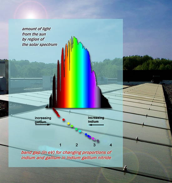
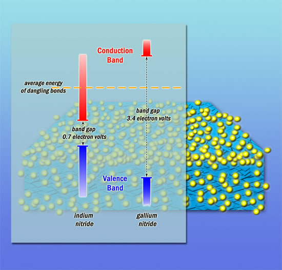
In 2002 Walukiewicz and his colleagues discovered that indium nitride has a remarkably narrow band gap, only 0.7 electron volts, which corresponds to the near-infrared region of the electromagnetic spectrum. The narrow band gap means that indium nitride could find applications in highly efficient light-emitting diodes, laser diodes, and high-frequency transistors. Even more promising, when alloyed with gallium nitride, another group III nitride (group III of the periodic table includes aluminum, gallium, indium, and other elements having three valence electrons), indium nitride holds out the possibility of making extraordinary solar cells. Gallium nitride has a band gap of 3.4 electron volts, matching the high energy of the near-ultraviolet region of the spectrum. Thin layers of indium, gallium, and nitrogen alloyed in different proportions could be stacked in a solar cell that would span virtually the entire spectrum of sunlight, yielding a solar cell far more efficient than any yet made. When electrons get in the wayWhat makes indium nitride frustrating, however, is that most semiconductor devices require two types of the material to form a junction, an n‑type that conducts negatively charged electrons and a p-type that conducts positively charged "holes." These types are usually made by "doping" the native material with impurities, either elements that donate electrons or those that accept electrons and leave behind holes. It's almost too easy to make n‑type indium nitride — even native, undoped InN is n-type — but it has proved almost impossible to make the p‑type. Until now. "Indium nitride is unique; it likes to be n-type," says Walukiewicz, not least because its peculiar electronic structure requires an unusual amount of energy to move the electrons out of its conduction band and make way for holes. The reason is that indium nitride crystals are riddled with defects, as many as tens of billions per square centimeter. Lots of atoms in these defects are unable to form bonds with their absent neighbors, and because the energy level of the defects lies right in the middle of InN's conduction band — which is what makes InN unique — these dangling bonds are all too eager to donate spare electrons to the conduction band.
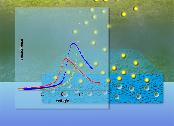
Moreover, says MSD team member Joel Ager, "Dangling bonds are found on the surface of indium nitride, where they create an n‑type accumulation layer impervious to chemical or physical treatment." The result, says team member Kin Man Yu of MSD, "is that you can't make an electrical contact with the bulk of the material, below the surface. Even if the bulk was p-type, you can't reach it because you can't get past the n-type surface layer." Adds Walukiewicz, "The surface if InN is by definition a highly conducting n-type semiconductor. You can't get through it by thinning it or etching it away; the n-type layer just reforms wherever you provide a new surface." Reaching into the interiorNevertheless, it should be possible to positively dope InN with an acceptor element. Magnesium has one less valence electron than indium and readily accepts electrons, leaving behind positively charged holes; as the only acceptor that works well in gallium nitride, magnesium may be the only one that works with InN as well. Using molecular beam epitaxy, William Schaff and his associates at Cornell University made several samples of magnesium-doped indium nitride and sent them to Berkeley Lab, where the MSD researchers used a form of mass spectrometry to measure the magnesium concentration in the samples. "We knew what the concentration was," says Yu, "but we really didn't know where it was or what it was doing." The challenge was to prove that the magnesium atoms had created p-type material in the bulk of the InN, even though the charge was masked by the negative surface accumulation layer. Says Ager, "A common method of measuring charge in a semiconductor is watching how the capacitance changes with changes in voltage — it changes one way with n-type material, the other way with p‑type. To make a capacitance voltage measurement of bulk InN, we had to get rid of the n-type layer." The way to do that with most materials is to apply voltage using a positively charged metal electrode through an insulating layer, "but we would have needed a huge electric field," Walukiewicz says. "It occurred to us we could use a liquid electrode — an electrolyte — instead."
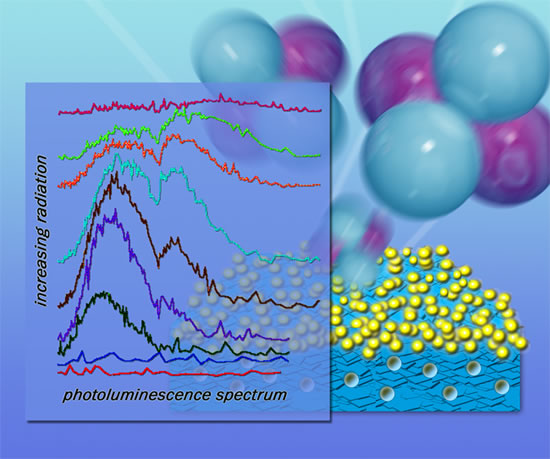
By forming a contact between the samples and a sodium hydroxide solution, the researchers formed a bilayer barrier, which acted much as a solid insulating layer would in normal capacitance voltage measurements. "As we increased the voltage, it removed electrons from the surface and gave us access to the bulk," Walukiewicz says. "We were able to see evidence of holes below the surface layer, beginning about six nanometers down." He says, "We were surprised that electrolyte capacitance voltage worked so well, but now it seems logical." Ager says that while this evidence of p-type conductance beneath the ubiquitous n-type surface was encouraging, "we knew that skeptics would demand additional verification." More proof of the p-typeThe researchers reasoned that they could create additional defects in the bulk of the p-type material by irradiating the samples with energetic particles; the defects would donate more electrons through dangling bonds and gradually destroy the material's positive conductance — in effect filling the holes created by the magnesium impurities. They bombarded both doped and undoped samples with two-million-electron-volt helium ions in controlled steps. In undoped samples, negative conductivity increased smoothly and proportionally, as the radiation created more electron donors in the form of defects with dangling bonds. But in doped samples the behavior was quite different: negative conductivity increased much more slowly at low radiation doses. At high doses, however, electrical activity of the magnesium acceptor atoms was eventually overwhelmed by the flurry of additional donor defects, and the electrical behavior of the samples soon began to resemble indium nitride that had never been doped. Photoluminescence — light emission after exciting the sample with a laser — also changed with step-wise increases in the radiation dose, as holes in the doped samples were displaced by electrons. Undoped InN samples all exhibited distinct photoluminescence signals (until subjected to massive radiation doses); by contrast, the magnesium-doped samples at first exhibited none. But with increasing doses, and an increasing proportion of negative electrons to positive holes, photoluminescence in the doped samples appeared and increased, until finally falling off at very high doses.
Ager says, "Proving that our doped samples were p-type is a major step forward — some semiconductors, like zinc oxide, can't be doped at all. But plenty of challenges remain." One challenge is the problem of the surface accumulation of negative charges that shields positively doped InN from electrical contact. The difficulty depends partly on the application; for solar cells made of indium-gallium-nitride alloys, possible solutions may lie with the nature of the alloys themselves. While Berkeley Lab researchers and their collaborators have a head start, first in establishing the potential of group III nitrides, then in seeing the promise of indium gallium nitride alloys in particular, they are not the only groups racing to meet challenges to practical applications; Walukiewicz says groups in Japan, France, Korea, and, closer to home, Santa Barbara "offer serious competition." "But we're optimistic," Walukiewicz says. "Otherwise we wouldn't be doing this." Members of the team reporting p-type doping of indium nitride include Kin Man Yu, Wladek Walukiewicz, and Joel Ager of Berkeley Lab's MSD, Becca Jones, Sonny Li, and Eugene Haller of MSD and the University of California at Berkeley's Department of Materials Science and Engineering, and Hai Lu and William Schaff of Cornell University's Department of Electrical and Computer Engineering. Research at Berkeley Lab was supported by the Office of Science of the U.S. Department of Energy; some team members have also been supported by the U.S. Department of Defense and the National Science Foundation. Additional information
|
||||||||||||||||||||
| Top | ||||||||||||||||||||