| July 26, 2006 | science@berkeley lab | | lab a-z index | lab home |
|
|||
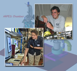
| Metal-to-Insulator Alchemy at the Advanced Light Source | ||||||||||||||||||||
| Contact: Lynn Yarris, lcyarris@lbl.gov | ||||||||||||||||||||
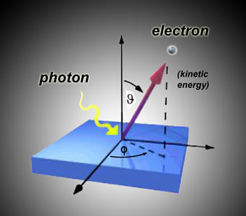
When an action on one electron in a solid material causes an effect on another, the two electrons are said to be "correlated." Electron correlation is expected to play a major role in spintronics and other technologies of the future, but first scientists need a much better understanding of correlated materials. A step in that direction was recently taken by a team of researchers working at Berkeley Lab's Advanced Light Source (ALS), one of the world's premier scientific sources of x‑rays. Using a technique called ARPES, for angle-resolved photoemission spectroscopy, the researchers were able to observe a material with strongly correlated electrons undergo a surprising transition from metallic electrical conductor to nonmetallic insulator.
The team was led by Kai Rossnagel and Lutz Kipp of the University of Kiel in Germany and included Neville Smith, Eli Rotenberg, and Hoon Koh of the ALS. The researchers doped the surfaces of samples of the transition metal tantalum disulfide (TaS2) with rubidium atoms, an alkali metal. The process should have transformed the sample into an increasingly more proficient metallic conductor; instead, with increased adsorption of the rubidium atoms the samples became more insulating. "TaS2 is a member of a large family of layered compounds called transition metal dichalcogenides, and we have done alkali adsorption experiments on quite a few of them. In all other cases alkali adsorption led to metallic compounds with higher conduction-electron densities, or to semiconducting compounds being turned into metals," says Rossnagel. "Only TaS2 became more insulating." Today's electronics industry is built on the freedom of negatively charged electrons to move in a current through a metal or metallic compound. But electrical charge is only one of three major properties of an electron in a solid material. In the future the electron's other two properties, its spin (described as being oriented up or down) and its orbital (which may be viewed as the shape of an electron in a solid), could also be exploited through the controlled response of electron correlation to external stimuli. "The cooperative response of correlated electrons to tiny changes in external stimuli such as stress, electric and magnetic fields, or photoexcitation results in dramatic changes of electrical, optical, or magnetic properties that could be exploited," says Rossnagel. Correlated electron effects include such phenomena as high-temperature superconductivity, colossal magnetoresistance, and metal-insulator transitions. Future devices that exploit these phenomena fall under the collective rubric of correlated electron technology, or CET. Structure begets functionThe surprising transition of the TaS2 samples -- from metal to insulator, when doped with rubidium -- came about because of the unique layer structure of TaS2. According to theory, the addition of the rubidium atoms should increase the spacing between the layers of TaS2 atoms in the material's crystal lattice, creating an electron structure that permits the conduction of electricity. What actually happened was that as the rubidium atoms were intercalated in the gaps between the layers, the electronic structure, as the result of correlated effects, was reconfigured so that it broke down conduction. "Because electron–electron interactions appear to be the dominant factor behind the metal-to-insulator transition we observed in our TaS2 studies with rubidium, we think it could be an ideal test system for studying this aspect of electron correlation," says Rossnagel.
The research was carried out at ALS Beamline 7.0.1, a spectromicroscopy beamline that uses an undulator magnet to generate x-rays in the energy range of 60-1200 electron volts, ideal for ARPES-based studies. The experimental end station the scientists used is called the Electronic Structure Factory and provides capabilities for making photoemission movies, capabilities used by Rossnagel and his collaborators. "Our photoemission movie was recorded during the deposition process and shows the evolution of the valence spectra as a function of deposition time," says Rossnagel. "At the beginning of the movie, the high spectral intensity near the highest occupied electron energy, the Fermi energy EF, identifies TaS2 as a metal. Then rubidium deposition is started, and spectral weight is continuously removed away from EF, gradually transforming the material into an insulator." In future studies, Rossnagel would like to change the species of alkali atom used in the adsorption experiments. If the increased separation of TaS2 layers from the intercalation of rubidium is responsible for the resulting metal-insulator transition, then an alkali atom smaller than rubidium, such as potassium, should make TaS2 less insulating. On the other hand, cesium, which is larger than rubidium, should make TaS2 even more insulating. Additional information
|
||||||||||||||||||||
| Top | ||||||||||||||||||||