| December 14, 2000 |
|
 |
 |
 |
||
|
|
Challenge: the chips in today's desktop
PCs are built up from more than a dozen layers of material etched with
electronic circuits. Each needs its own photomask to project the circuit
pattern. How much time and expense could be saved if no masks were
necessary?
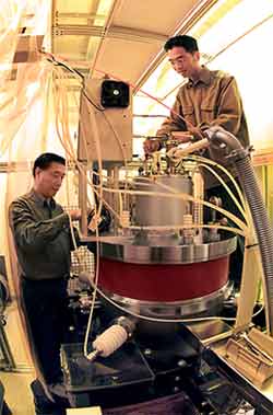
Challenge: to adjust electronic properties, precise amounts of impurities ("dopants") must be introduced at different locations in the layers, often using ion beams to implant the dopants. What if the same beams that implant the ions could carve the layers of circuitry? Challenge: today's chips contain millions of elements with features as small as a fraction of a micrometer (millionth of a meter), projected by visible light. To pack in more elements, smaller features are needed. What's the best technique for defining features smaller than a wavelength of visible light? Ka-Ngo Leung of Berkeley Lab's Accelerator and Fusion Research Division (AFRD) is addressing these and other questions with ion-beam technology. "Chip manufacturers hope to pack a hundred million transistors on a chip by 2005," says Leung, who is head of AFRD's Plasma and Ion Source Technology Group and a professor in the Nuclear Engineering Department at the University of California at Berkeley. "In five years or so, features as small as 100 nanometers will be common. We're shooting for 50 nanometers" -- 50 billionths of a meter. Ions, usually atoms lacking one or more orbiting electrons, are particles with net electrical charge; they can be steered by electric and magnetic fields. All particles have an associated wavelength, and the equivalent wavelength of a typical ion beam is more than a million times shorter than visible light. Depending on the atomic species, ion beams can be used to dope semiconductors even as they carve out circuit patterns. What's more, by using what Leung calls "dot-matrix on the nanoscale," he and his colleagues intend to use ion beams to do away with conventional lithography masks altogether. Working with Tsu-Jae King, an associate professor of electrical engineering and computer science at UC Berkeley, and with graduate students Quing Ji, Vinh Van Ngo, and Karen Scott, Leung built the Maskless Microbeam Reduction Lithography system (MMRL) recently inaugurated by Berkeley Lab director Charles Shank and David Patterson of the Defense Advanced Research Projects Agency, sponsor of the project. In the MMRL, an ion source accelerates ions at precisely controlled energies through a "universal pattern generator," an array of fine holes, each a micrometer in diameter, in a compound electrode 40 micrometers thick. Each hole forms an ion beamlet which can be switched on or off to create any desired pattern. Instead of a dozen separate masks, a dozen different patterns can be programmed to quickly succeed one another. The MMRL's ion source produces ions with an energy of some 20 electron volts (20eV), compared to the whopping 10,000 electron-volt energies (10keV) required by the MMRL's European competitor, an ion-lithography device made by a consortium headed by Infineon Technologies. The pattern of beamlets that emerges from the MMRL's pattern generator is focused down and reduced 10 times before it reaches the target wafer, compared to four times for the Infineon machine and others. "Presently we reduce the pattern 10 times to achieve features of 100 nanometers," says Leung. "Soon we'll reduce it 20 times or more for 50-nanometer and smaller features." He adds that "by using a multiplexing scheme, we've also simplified the pattern generator. Instead of one wire to each hole -- that's a lot of wires! -- we control the array by wiring the holes together along the x axis in one layer and wiring them together along the y axis in a separate layer. For nine holes, that's only six wires; for 100 holes, only 20 wires -- in other words, we only need x-plus-y wires, not x-times-y wires." Using a separate Focused Ion Beam (FIB) lithography system, Leung and King have precisely focused and scanned ion beams using lenses comprised of multiple electrodes. They are demonstrating "direct-write" processes with beams of oxygen, boron, and phosphorus, inscribing patterns directly on movable substrates or selectively doping the substrates. By using several beams at once, Leung's group can achieve much faster processing and higher "throughput," making progress toward a practical industrial process. By combining the multiple-beamlet array of the MMRL with individual FIB beamlets, Leung hopes to produce an even more versatile machine, the Maskless Nanobeam Lithographer, in which self-focusing beamlets can produce "dot matrix" arrays and can also be used with moving substrates, allowing patterns to be inscribed without distortion on very large flat substrates -- and on curved surfaces as well. Ion beam lithography is one of several responses to the challenges posed by Moore's Law, the assumption that the density of devices on a chip will double roughly every year and a half. Other techniques to keep this so-called "law" in force as long as possible are also being developed at Berkeley Lab, including using electron beams and extreme ultraviolet light to project mask patterns onto the wafer. "Resist" layers and subsequent etching are needed to transfer mask patterns in this way, however. One of the unique features of ion beams is their ability to define features without using resists. "Of all the types of particles -- photons, electrons, ions -- which are employed in lithography, ions have the shortest effective wavelength," says Tsu-Jae King, "so that in principle they achieve the smallest features." AFRD's Plasma and Ion Source Technology Group is taking advantage of the special nature of ions in machines which are among the leading contenders for the next generation of integrated-circuit lithography technology. Additional information: |