|
January 26, 2000 |
|
 |
 |
 |
||
|
|
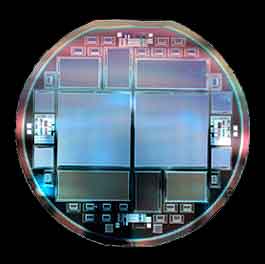
Berkeley Lab's Steve Holland, an electrical
engineer in the Physics Division's microsystems laboratory, has pioneered
a new class of photodetectors with origins in high-energy physics. These
ingenious detectors have already found novel applications in medical
diagnosis and are now poised to look into the far reaches of the cosmos.
Michael Levi, who heads the Physics Division's program to develop CCDs (charge-coupled devices) based on the new technology, says the potential applications include an astronomical CCD with unprecedented efficiency in the infrared region of the spectrum; an x-ray imager responsive at photon energies with greater dynamic range than those on the Chandra X-ray Observatory satellite -- and potentially useful in mammography as well; and even a new generation of particle detectors. Says Levi, "The new CCD would give ten times better resolution than some of the silicon vertex detectors presently in use that were pioneered at Berkeley Lab. From this heritage of particle-detector work for high-energy physics, a unique new CCD has emerged with tremendous potential for many fields of science and medicine." Indeed, at a recent Physics Division review, noted astronomer Joel Primack of UC Santa Cruz voiced the opinion that "these CCDs will transform astronomy." CCDs are semiconductor devices that convert patterns of light into patterns of electric charge, which can be recorded and computer-processed to form images (they also pinpoint hits by energetic particles). The new CCD's spectacular advantages for astronomy are a direct result of its particle-detector ancestry. "The new CCD is truly a spin off of high-energy physics detector work," says Steve Holland, "and had its origin in the R&D effort for the Superconducting Supercollider." A typical particle detector is a slab of silicon 300 micrometers thick, about the thickness of a postcard. By comparison, to register dim blue light, most astronomical CCDs have to be thinned to less than the width of a human hair. Not only is a thin chip fragile, it sacrifices sensitivity to red and infrared light. The designers of the Berkeley Lab CCD, however, found a way to use thickness to advantage, retaining blue sensitivity while vastly improving response in longer wavelengths. Commercial CCDs, such as those used in consumer cameras and video recorders, are front-illuminated; incoming photons must pass through or around circuitry on the front to reach a thin layer underneath where electrons are produced. These charges are collected in "potential wells" which are read and emptied periodically. For astronomical CCDs the circuitry blocks too much blue light, so they must be back-illuminated. Nearly the entire substrate must be mechanically and chemically removed so that photon-generated charges can reach the potential wells, leaving only a 20-micron thin layer beneath the circuitry. So many of these gossamer chips are damaged during fabrication that the survivors are worth tens of thousands of dollars apiece. "Steve wanted to make a CCD that could go straight off the wafer and into the telescope," says Donald Groom of the Physics Division, who is helping to develop the astronomical CCD. "The first step was to make a back-illuminated chip that was sensitive to blue light without thinning." The method Holland devised depends on using very pure, negatively doped (n-type) silicon. Electrically active dopants in this kind of silicon amount to only about one part in a hundred billion; special care is required during fabrication to maintain this level of purity. "In our high-energy work we had developed a unique combination of techniques for 'gettering' -- getting rid of impurities -- to produce detectors with low dark current," Holland explains. Dark current is caused by charges not created by incoming photons, but by thermal energy in the material itself. Another important feature of Holland's design is that the silicon is fully depleted. "By layering a thin, transparent window onto the back of the n-type silicon substrate -- a window that also acts as an electrode -- we can apply a bias voltage between the window and the positively doped channel layer under the front circuitry." The voltage fully depletes the substrate's charge density -- that is, it clears the silicon of charge carriers. Such material is called high-resistivity silicon. The result is that when a photon of blue light produces an electron near the back surface of the chip, the electron can travel all the way through to the front layer without being lost to recombination. Spatial resolution is good, because the electrons accurately reflect the position of the photons that produced them. In blue light, the 300-micrometer-thick, fully-depleted chip electronically mimics a thin chip. In red light, the thick chip does much better than a thin one. A thick chip has much more material in which the long-wavelength photon can interact. Unlike a thin chip, in which red light is reflected back and forth between the front and back surfaces, producing interference fringes -- a particular problem for astronomers who study very distant, highly redshifted objects -- in a thick chip under voltage the charge carriers travel nearly straight to the potential wells, with little sideways diffusion; no fringes are produced by reflection. In tests at the Detector Development Laboratory at the University of California's Lick Observatory, a new CCD with four million pixels has shown remarkable response to red and infrared light; indeed, in the near-infrared it has shown better quantum efficiency -- the ratio of incoming photons converted to electric charge -- than any astronomical CCD now in use. Because the CCDs are used "backside-up," the circuitry is hidden, and their light-sensitive surfaces can fit side by side to form very large arrays. An eight-million-pixel CCD is being fabricated for spectroscopy at the giant Keck telescope; another proposal, by the international Supernova Cosmology Project based at Berkeley Lab, would put a CCD camera with more than 200 such chips in a satellite dubbed SNAP, for SuperNova/Acceleration Probe. "SNAP's optical imager will have nearly a billion pixels, the largest and most sensitive astronomical imager ever fabricated," says Michael Levi, who with Saul Perlmutter is the SNAP satellite's co-principal investigator, noting that "the high redshift of distant supernovae makes the new CCD essential to the undertaking." Says Holland, "Fabricating an astronomical CCD turns out to be enormously more complex than fabricating high-energy particle detectors. High-energy silicon detectors require only three masks for ion implantation, wiring, and electrical contact to the implanted regions. The astronomical CCD requires 10 masks, very accurate registration between layers, and three layers of silicon for the electrodes. The masks are about eight times as expensive, too." Most of the CCD fabrication is done at Berkeley Lab's Microsystems Laboratory, a facility originally developed to support the Superconducting Supercollider. "Thanks to the careful planning that went into the development of the Microsystems Laboratory, which is managed by Nick Palaio of the Engineering Department, we were able to take on this difficult task." Holland, Groom, and their colleagues were greatly helped in obtaining finished mask designs and other design aspects by consultation with Richard Stover, Mingzhi Wei, Kirk Gilmore, and Bill Brown of the Lick Observatory's Detector Development Laboratory and with James Janesick, formerly of the Jet Propulsion Laboratory, now Executive Vice President of Pixel Vision, Inc. With help from UC Berkeley, Nick Palaio secured a donation of lithography equipment from Intel Corporation, necessary for fabricating the CCD tested at the Lick Observatory. New equipment to facilitate CCD production has been made possible by a recent grant from the California Association for Research in Astronomy (CARA), a partnership of the University of California and the California Institute of Technology. Additional Information: |