|
August 11, 2000 |
|
 |
 |
 |
||
|
|
Tiny, sturdy, and far more energy-efficient
than incandescent lamps, light-emitting diodes (LEDs) are already widely
used in traffic stoplights, vehicle brake lights, and big animated signs.
Other uses, including cool, economical home and commercial lighting, are
on the way -- it's a big business that's getting bigger all the time.
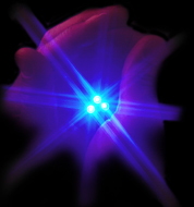
Until the 1990s, LEDs were limited to longer wavelengths, from the far infrared through red to green. Then scientists at Meijo University and Nichia Chemical Industries in Japan found a way to use thin films of gallium nitride and related materials on a substrate of sapphire to produce blue light. Brighter greens, blues, violets, and even ultraviolet light were soon shining from LEDs made with such materials. Their design and manufacture, however, posed persistent problems. Fundamental scientific questions had not been answered. Joel Ager, Eugene Haller, Wei Shan, and Wladek Walukiewicz of Berkeley Lab's Materials Sciences Division (MSD), working with colleagues at Hewlett-Packard -- now Agilent Technologies -- and Xerox, have overcome two important barriers to the economical manufacture of these new solid-state light sources. In separate investigations, they have learned what causes destructive cracking in an essential component of the diodes, and they have learned how devices made with gallium nitride alloys can emit light efficiently despite being plagued by numerous structural defects. How LEDs do it Near room temperature, the valence electrons of a pure semiconductor such as gallium nitride are locked up in chemical bonds -- the valence band is filled with electrons, and the conduction band is practically empty. Because there is an energy gap between these bands (the amount of energy, characteristic of each different material, needed to kick an electron out of the valence band up into the conduction band), there are no mobile charges, and the material is insulating. Charge carriers can be provided by "doping" a semiconductor with atoms that have more or fewer electrons than the atoms of the host. Dopants that add negatively charged electrons to the conduction band create n-type material; those that allow "holes" to form in the valence band create p-type material. If p-type and n-type regions meet at a junction, the structure is a diode. In a diode, when electrons from the n-type region "recombine" with holes in the p-type region (or vice versa) they release energy, which takes the form of heat in some materials and light in LEDs. The wavelength of the light is determined by the band gap of the emitting material. "The conditions for radiative recombination -- emitting light -- are, first, a direct bandgap, so the electrons and holes recombine efficiently; second, a material that is low in defects, preferably defect-free, so the recombination energy is not dissipated as heat; and finally, a supply of holes and electrons injectable from p and n regions," says Eugene Haller. The hows and whys of indium gallium nitride In the 1950s it was discovered that all the direct bandgap semiconductors combine one or more elements from group III of the periodic table, such as gallium, with one or more from group V, such as arsenic. LEDs made from gallium arsenide and its alloys became available in the 1960s, but the direct bandgaps of conventional group III-V semiconductors covered only the spectral range from red to amber, leaving much of the visible spectrum beyond the reach of LEDs. "There were early efforts to make LEDs from gallium nitride, which has a bandgap of 3.4 eV and emits ultraviolet light, but it was very hard to grow and there was no method of doping it to get p-type material," Haller says. "Then, in the late '80s, Isamu Akasaki, Shuji Nakamura, and their colleagues learned how to grow n- and p-doped thin films of gallium nitride on sapphire. The basic pieces of the puzzle were in place." Daunting problems remained. The gallium nitride compound itself emits pure ultraviolet light; to get violets, greens, and blues, it has to be alloyed with indium nitride in the right proportions, to reduce the band gap. Because the various alloys each have slightly different lattice parameters, strain results when multilayered structures are grown, and defects form. "What kills light emission is when electrons or holes are trapped, as in defects, and lose energy to nonradiative processes -- to heat," says Wladek Walukiewicz. Generating light is a constant competition between radiative recombination, an intrinsic property of the material, and the nonradiative processes imposed by different kinds of defects and their concentrations. "The prescription for efficient light emitters is to help the radiative side of the competition by eliminating or at least reducing the concentration of defects," Walukiewicz says. "There are a huge number of defects in gallium nitride compounds -- a hundred million to ten billion per square centimeter," says Haller. "If gallium arsenide crystals had as many defects as gallium nitride compounds, no photons could escape. The LEDs would remain completely dark! People were asking themselves how diodes made with gallium nitride alloys, with so many defects, could even work."
In fact, indium gallium nitride devices can emit colors all the way from visible red to ultraviolet, which has made these compounds very attractive. But different groups attempting to make the same material got widely varying results: different colors of light, different efficiencies, different temperature stabilities, and so on. To resolve these puzzling results, the MSD team studied light emission from small samples of different alloys in a diamond anvil cell, systematically squeezing them to pressures like those deep within the Earth, at temperatures down to four degrees above absolute zero. "We didn't make diodes, we just illuminated indium gallium nitride samples, the essential part of the diodes, with a laser and studied what kind of light we got out," says Walukiewicz. "This allowed us to plot variations in the energy gap of the materials as a function of pressure and temperature and to elaborate on the nature of the electronic states participating in the light emission." The results were intriguing. The team found that indium mixes unevenly with gallium nitride, and in very small areas where indium is concentrated, the band gap is less than the average for the material as a whole. In these small regions, light-emission intensity is higher. Because they are small, numerous, and distributed throughout the material, indium-rich regions produce light efficiently even though the crystal is riddled with defects. Haller says, "Through these studies we were able to gain a significant understanding of how the bandgap is modulated through compositional variations in these materials." Preventing cracks A different problem in the manufacture of LEDs made with gallium nitride is that large cracks develop in gallium nitride films doped with silicon, which is used for the n-type base structure of the devices. "Gallium nitride films are vapor-deposited on sapphire at a temperature of 1,000 degrees Celsius," explains MSD's Joel Ager. Sapphire, crystalline aluminum oxide, "is a good substrate because it can take the high temperature, but its lattice constant and thermal-expansion coefficient are not well matched to gallium nitride." This results in stress. Even so, gallium nitride not doped with silicon resists cracking. Indeed, Walukiewicz points out that "gallium nitride is very strong, very mechanically stable, and has a large heat capacity. You can run it red hot." Adding silicon makes a drastic difference. "You need a fairly thick n-type layer at the bottom of the stack in a multilayer device," says Ager, "but at high thickness and high silicon concentration, the gallium nitride layer shatters like ice." Yet silicon atoms themselves do not appreciably distort the crystal structure of gallium nitride or change its response to heat. What difference could doping with silicon -- typically only one part in a thousand -- make? The team made a systematic study of stress in films, grown by Hewlett-Packard and Xerox, with a wide range of thicknesses and silicon concentrations. Stress was measured by several complementary methods: optical studies at Berkeley Lab, electron microscopy at Xerox, and x-ray diffraction at both Hewlett-Packard and Xerox. Eventually a consistent picture emerged. "It turns out that silicon changes the growth mechanism," says Ager. "In gallium nitride doped with silicon, as the layer grows, it creates tensile stress," which pulls flaws open. "The thicker the layer grows, the greater the stress. Eventually a flaw of sufficient size will cause a crack to develop, and the layer will rip itself apart." Growth by vapor deposition is always at the surface of the material, and silicon changes the way gallium and nitrogen react on the surface. With this information, Hewlett-Packard was able to change growth conditions to produce large gallium nitride devices more economically. "By cooperative work between Berkeley Lab, HP, and Xerox, we untangled a very subtle but important problem," says Ager. "It's a pleasure to have access to real problems in industry that will have a substantial impact on our way of life." Additional information:
|