April 12, 1999 |
|
 |
 |
 |
||
| BERKELEY, CA. -- In 1905, one of the papers
that brought Albert Einstein international recognition was his explanation of the puzzling
photoelectric effect: depending on its frequency, light falling on metal
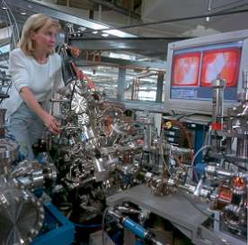
can stimulate the emission of electrons and a flow of electricity. How? Light is quantized, Einstein proposed; the energy of the quantum (later named a photon) depends on the frequency of the light, and a quantum of the right energy boosts an electron out of its orbit. The same phenomenon makes the PEEM2 at the Advanced Light Source (ALS) -- a new photoemission electron microscope recently commissioned on beamline 7.3.1.1 -- a powerful tool for studying materials: their structures, elemental make-up, chemical bonds, the orientation of their molecules, and their magnetic properties.
X-rays or extreme ultraviolet light produced by the ALS can be tuned to knock copious amounts of electrons out of a sample. PEEM2 focuses the emitted electrons on a phosphor screen, and the visible-light image produced this way is aquired by a charge-coupled- device camera (CCD) with a resolution of 20 nanometers (billionths of a meter) -- more than ten times better than the resolution of the best optical microscopes. PEEM2 accepts samples up to 15 millimeters wide and can be fitted with any one of four changeable apertures, from as wide as two millimeters to as narrow as 12 microns. "The narrowest aperture gives the highest resolution," explains Simone Anders, leader of the team in the ALS Experimental Systems Group, headed by Howard Padmore, which designed the microscope, "but there’s a trade-off between resolution and electron transmission." In a photoemission electron microscope, the x-ray spot illuminating the sample is wider than the microscope’s field of view, and the resolution is limited only by the focusing system. PEEM2’s four electrostatic lenses focus the image at variable magnification. A typical exposure time is several seconds, although the CCD can capture up to four images a second. A high-vacuum preparation chamber allows sample preparation right at the PEEM2 end-station. Inside the vacuum chamber, thin films and multilayer structures can be grown; samples can be cleaned by sputtering and characterized using such standard techniques as low-energy electron diffraction, and they can also be heated to 1500 degrees C before being carried into the beam line on a motorized rod. PEEM2 combines the traditional features of photoemision electron microscopy, including the ability to determine surface topography, with such spectrographic techniques as Near Edge X-ray Absorption Fine Structure (NEXAFS) spectroscopy, which is practical only with synchrotron radiation. In NEXAFS, an x-ray photon excites an electron orbiting the core of an atom or molecule to leave its orbit and jump to a higher energy level. The step-like vertical rise in a graph showing the absorption intensity as a function of the energy of the x-ray is called an "edge;" for each electron orbital the position of the edge differs according to the individual element, chemical bond, or molecular orientation. Tuning radiation to different frequencies can thus produce spectrographic information which becomes part of the visual image, revealing just where in the sample certain elements or certain kinds of chemical bonds occur. Because it uses light from a bending magnet, PEEM2 can do more. The beam leaving a bending magnet can be masked to emit either linearly polarized light, or right or left circularly polarized light. Linearly polarized light is useful to determine the orientation of bonds in thin films, for example. Magnetic regions of a sample exhibit a phenomenon known as circular dichroism, the difference in their absorption of right and left circularly polarized light; a magnetic contrast is visible because of the different interaction of the spin of the radiation with magnetic domains of opposite orientation. With a beam tuned to a characteristic absorption edge of a magnetic material such as cobalt, PEEM2 can look at the surface of a computer disk, for example, and distinguish the orientation of its innumerable magnetic bits with high resolution. "PEEM2 can even distinguish the magnetic properties of individual layers in multilayer structures," says Anders. "Magnetic multilayers may soon be used in magnetic memories, replacing electronic memory chips for various applications." She lists other examples of the kind of research pertinent to the future of the electronics industry: "Because it can distinguish between chemical bonds, PEEM2 can map areas of predominately diamond-like bonds versus areas of graphite-like bonds in thin films of amorphous carbon, which are of potential use in flat-panel displays. And because PEEM2 can distinguish molecular orientations, it can be used to examine the mechanisms of polymer alignment." Aligned polymer thin films are important components of liquid crystal displays. "The strength of PEEM2 is that no other microscope can do all this," Anders says. "That’s one of the reasons why the Department of Energy entered into a CRADA" -- a Cooperative Research and Development Agreement -- "with IBM to build and use it at the Advanced Light Source." Anders and her coworkers, including Joachim Stöhr of IBM, Michael Scheinfein of Arizona State University, and a team of ALS engineers led by Ron Duarte, constructed PEEM2 over a three-year period and have been its principal users, but beginning in February of 1999, half the beam-time of the microscope and its beamline will be available to qualified outside users. Meanwhile Anders and her colleagues are advancing further toward the high-resolution frontier with a design for an even higher resolution instrument, the PEEM3. |