| lab a-z index | phone book |
| July 19, 2007 | news releases | receive our news releases by email | science@berkeley lab |
|
|||
|
|||
Berkeley Researchers Find New Way To Fabricate Striped Nanorods |
||||||||||||||||
| News contact: Lynn Yarris (510)486-5375 or lcyarris@lbl.gov
Scientific contact: Paul Alivisatos, alivis@berkeley.edu |
||||||||||||||||
BERKELEY, CA — Superlatticed or “striped" nanorods – crystalline materials only a few molecules in thickness and made up of two or more semiconductors – are highly valued for their potential to serve in a variety of nanodevices, including transistors, biochemical sensors and light-emitting diodes (LEDs). Until now the potential of superlatticed nanorods has been limited by the relatively expensive and exacting process required to make them. That paradigm may be shifting.
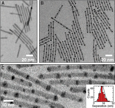
A team of researchers with the U.S. Department of Energy’s Lawrence Berkeley National Laboratory (Berkeley Lab) and the University of California (UC) at Berkeley, has found a way to make striped nanorods in a colloid – a suspension of particles in solution. Previously, striped nanorods were made through epitaxial processes, in which the rods were attached to or embedded within a solid medium. “We have demonstrated the application of strain engineering in a colloidal quantum-dot system by introducing a method that spontaneously creates a regularly spaced arrangement of quantum dots within a colloidal quantum rod,” said chemist Paul Alivisatos who led this research. “A linear array of quantum dots within a nanorod effectively creates a one-dimensional superlattice, or striped nanorod.” Alivisatos is an internationally recognized authority on colloidal nanocrystal research who holds joint appointments with Berkeley Lab and UC Berkeley. He’s the corresponding author on a paper published in the July 20, 2007 edition of the journal Science, reporting the results of this latest work. The paper is entitled: “Spontaneous Superlattice Formation in Nanorods Through Partial Cation Exchange.” Co-authoring the Science paper with Alivisatos were Richard Robinson, of Berkeley Lab’s Materials Sciences Division (lead author); Denis Demchenko and Lin-Wang Wang, of Berkeley Lab’s Computational Research Division; and Bryce Sadtler and Can Erdonmez, of the UC Berkeley Department of Chemistry. Today’s electronics industry is built on two-dimensional semiconductor materials that feature carefully controlled doping and interfaces. Tomorrow’s industry will be built upon one-dimensional materials, in which controlled doping and interfaces are achieved through superlatticed structures. Formed from alternating layers of semiconductor materials with wide and narrow band gaps, superlatticed structures, such as striped nanorods, not only can display outstanding electronic properties, but photonic properties as well. “A target of colloidal nanocrystal research has been to create superlatticed structures while leveraging the advantages of solution-phase fabrication, such as low-cost synthesis and compatibility in disparate environments,” Alivisatos said. “A colloidal approach to making striped nanorods opens up the possibility of using them in biological labeling, and in solution-processed LEDs and solar cells.” Previous research by Alivisatos and his group had shown that the exchange of cations could be used to vary the proportion of two semiconductors within a single nanocrystal without changing the crystal’s size and shape, so long as the crystal’s minimum dimension exceeded four nanometers. This led the group to investigate the possibility of using a partial exchange of cations between two semiconductors in a colloid to form a superlattice. Working with previously formed cadmium-sulfide nanorods, they engineered a cation exchange with free-standing quantum dots of the semiconductor silver-sulfide.
“We found that a linear arrangement of regularly spaced silver-sulfide contained within a cadmium-sulfide nanorod forms spontaneously at a cation exchange rate of approximately 36-percent,” said Alivisatos. “The resulting striped nanorods display properties expected of an epitaxially prepared array of silver-sulfide quantum dots separated by confining regions of cadmium-sulfide. This includes the ability to emit near-infrared light, which opens up potential applications such as nanometer-scale optoelectronic devices.” One of the key difference between quantum dots epitaxially grown on a substrate and free-standing colloidal quantum dots is the presence of strain. The use of temperature, pressure and other forms of stress to place a strain on material structures that can alter certain properties is called “strain engineering.” This technique is used to enhance the performance of today’s electronic devices, and has recently been used to spatially pattern epitaxially grown striped nanorods. However, strain engineering in epitaxially produced striped nanorods requires clever tricks, whereas Alivisatos and his colleagues discovered – through Ab initio calculations of the interfacial energy and computer modeling of strain energies – that naturally occurring strain in the colloidal process would be the driving force that induced the spontaneous formation of the superlattice structures. “This project has involved tight coordination between computer simulations and experiment, and the results obtained here would not have been possible to achieve without the contributions of our computational scientists, Demchenko and Wang,” Alivisatos said. “It is another clear example where we see that theoretical simulations are not just being used to explain materials growth after the fact, but are now an integral part of the materials designand creationprocess from the very start.” Even though the colloidal striped nanorods form spontaneously, Alivisatos said it should be possible to control their superlatticed pattern – hence their properties - by adjusting the length, width, composition, etc., of the original nanocrystals. However, much more work remains to be done before the colloidal method of fabricating striped nanorods can match some of the “spectacular results” that have been obtained from epitaxial fabrication. “For now, the value of our work lies in the unification of concepts between epitaxial and colloidal fabrication methods,” he said. Berkeley Lab is a U.S. Department of Energy national laboratory located in Berkeley, California. It conducts unclassified scientific research and is managed by the University of California. Visit our Website at www.lbl.gov. Additional Information
|
||||||||||||||||
| Top | ||||||||||||||||