|
May 12, 2003
|
||
|
 |
 |
| Gallium nitride makes for a new kind of nanotube | ||
| Contact: Lynn Yarris, lcyarris@lbl.gov | ||
|
|
To the growing list of nanosized objects created in a laboratory you can now add nanotubes synthesized from the prized semiconductor gallium nitride. A team of Berkeley Lab scientists has created gallium nitride nanotubes with diameters ranging between 30 to 200 nanometers. By comparison, a human hair has a diameter of about 100,000 nanometers.
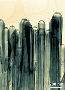
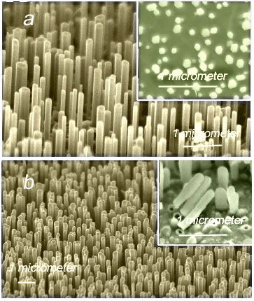
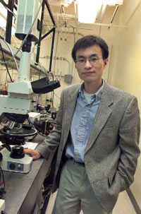
"These gallium nitride nanotubes are electronically and optically active and, because they're made from single crystals, exceptionally durable and uniform in their properties," says Peidong Yang, a chemist with Berkeley Lab's Materials Sciences Division and a professor with UC Berkeley's Chemistry Department who led this research. "They offer a wide range of opportunities for technological applications." Results of this research were published in the April 10 issue of the journal Nature. Coauthoring the paper with Yang were Yanfeng Zhang, Sangkwon Lee and Heon-Jin Choi of Berkeley Lab, and Joshua Goldberger, Rongrui He and Haoquan Yan of UC Berkeley. Gallium nitride is considered by many to be the next important semiconductor material after silicon. As a brilliant light emitter capable of operating at high temperatures, it is a leading candidate to be the key material for the next generation of high frequency, high power transistors. The major drawback to gallium nitride technology has been the cost of growing gallium nitride crystals. A relatively inexpensive means of mass-producing high-quality uniform gallium nitride nanotubes should create a lot of interest in the high-tech community. The gallium nitride nanotubes created by Yang and his "These nanotubes could mimic ion channels like those in a biological cell, or they could be used to separate molecules in the same way as the microscale labs-on-a-chip," he says. In 1991, Japanese chemist Sumio Iijima created hollow cylinders of carbon measuring only a billionths of a meter in diameter that he dubbed nanotubes. Carbon nanotubes created a big sensation in the materials sciences; ever since then researchers have sought to synthesize nanotubes from solids other than carbon, especially from semiconductors. While there has been some success along that direction, these tubes have either been amorphous or polycrystalline, which made them too fragile for practical use. Yang and his colleagues overcame this problem through the development of a fabrication technique Yang calls "epitaxial casting." It is based on a technique he and his group developed earlier to make "nanowire nanolasers," perhaps the smallest ultraviolet light-emitting lasers ever produced. The nanowires are made from pure crystals of zinc oxide that grow vertically in aligned arrays like the bristles on a brush. These zinc oxide "bristles" range from 2 to 10 microns in length, depending upon how long the growth process is allowed to proceed. Typically, millions of zinc oxide nanowires form on a sapphire wafer substrate over a period of about ten minutes.
For the gallium nitride nanotubes, Yang and his colleagues used the zinc oxide nanowires as templates over which they grew crystals of gallium nitride through chemical vapor deposition. Heat was then applied to evaporate away the zinc oxide cores -- gallium nitride being a much more thermally stable material – leaving only the gallium nitride sheaths, a high-density, ordered array of nanosized tubes. "Electron diffraction measurements showed that our gallium arsenide nanotubes are single crystals," Yang says. "To the best of our knowledge, this is the first example of the formation of single crystal gallium arsenide nanotubes." Scanning electron microscopy showed that the tubes Yang and his colleagues made were of uniform length, about two to five microns. Yang says that the epitaxial casting technique allows tube length to be controlled and that it should be no problem to grow tubes 20 or more microns in length. He also notes that while most of the tubes they produced remained attached to the sapphire substrate and were open at one end only, others broke off from the substrate and were open at both ends. This property of tubes being open at one or both ends is another factor that can be controlled, he says.
Yang says the epitaxial casting technique should also work for making nanotubes out of many other semiconducting materials as well. He and his group expect to incorporate their nanotubes into a device, such as a transistor or a sensor, in the near future. Additional information
|
||||||||||||||||||||||||||||||||||