|
June 4, 2002
|
|
 |
 |
| The race to make the next generation of semiconductor chips: extreme ultraviolet lithography leads the field | ||
| Contact: Paul Preuss, paul_preuss@lbl.gov | ||
|
|
(The race for extreme ultraviolet lithography, part 2) Meanwhile, back at the beamline... "The interferometer is wonderful for testing optics, but the proof of what the optics can do is in the printing," says CXRO's present director, Erik Anderson. He explains that "because high-coherence ALS light is ideal for interferometry but not for printing, Paul Denham and Patrick Naulleau developed a scanning illumination system that could fill the patterned mask area with a wide, programmable range of incident-angle EUV light. Using this scanning illuminator, we can produce almost any possible illumination pattern, which is very important in lithography research." The resulting device was called the SES, the "static exposure station" -- static because, unlike the full-blown ETS, it projects only a portion of a mask pattern and exposes only part of a wafer at a time.
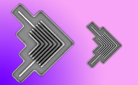
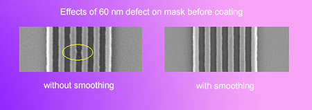
The actual chip-making performance of the optics was even better than they had been designed to achieve. Mirrors designed to make features with better than 100 nanometer resolution readily created 70 nm features. And by manipulating parameters like beam angles and exposure times, the CXRO team achieved much smaller features spaced just 39 nanometers apart. They also tested ways to get rid of defects in masks. "If there's a defect at the bottom of all those layers, you can't directly repair it. So the question is how to smooth it out." The team used the Nanowriter, CXRO's ultra-high-resolution electron-beam lithography machine, whose operations Anderson manages, to create masks with programmed defects. With the SES, they printed from these masks using different coatings developed at Livermore. Anderson says, "Coatings optimized for smoothing minimized the irregularities, like snow on grass. With nonsmooth coatings, the defects stood out like snow on a boulder."
By printing from the newest set of optics and special test masks, says Anderson, "we have verified the interferometry and demonstrated the impressive capabilities of EUV lithography." And as commercial chip manufacture draws closer, CXRO's EUV interferometer has another role to play. "We set the standard in interferometry, but for commercial use, the goal is get visible-light interferometry accurate enough so that at-wavelength interferometry won't be needed for EUV steppers used in routine manufacturer. In close collaboration with our partners at Livermore, who specialize in visible interferometry, our task is to help insure that the required accuracy is achieved." The size of things to come Meanwhile current photolithography techniques, which have already used deep ultraviolet light at 248 nm wavelengths to craft chips with line widths of only 80 or 90 nanometers, will be extended to 193 nm and possibly 157 nm wavelengths for making chips with line widths less than 70 nanometers. To make anything smaller than that, EUVL is essential. By 2007, commercial production of chips at the 45 nm "node" is expected to begin, using Intel's ASML beta machine. By 2009, capability will be extended to the 32 nm node, resulting in finished chips with 13 nm line widths or less. Computers using the first EUVL-made chips are expected to have ten times
the speed and ten times the memory of today's machines. That will be just
the beginning of the next generation of superdense integrated circuits.
|
||||||||||||||